
The history of storage devices is quite literally a race between the medium and the computing power as the bottleneck of preserving billions of ones and zeros stands in the way of computing nirvana. The most recent player is the Non-Volatile Memory Express (NVMe), something of a hybrid of what has come before.
The first generations of home computers used floppy disk and compact cassette-based storage, but gradually, larger and faster storage became important as personal computers grew in capabilities. By the 1990s hard drive-based storage had become commonplace, allowing many megabytes and ultimately gigabytes of data to be stored. This would drive up the need for a faster link between storage and the rest of the system, which up to that point had largely used the ATA interface in Programmed Input-Output (PIO) mode.
This led to the use of DMA-based transfers (UDMA interface, also called Ultra ATA and Parallel ATA), along with DMA-based SCSI interfaces over on the Apple and mostly server side of the computer fence. Ultimately Parallel ATA became Serial ATA (SATA) and Parallel SCSI became Serial Attached SCSI (SAS), with SATA being used primarily in laptops and desktop systems until the arrival of NVMe along with solid-state storage.
All of these interfaces were designed to keep up with the attached storage devices, yet NVMe is a bit of an odd duck considering the way it is integrated in the system. NVMe is also different for not being bound to a single interface or connector, which can be confusing. Who can keep M.2 and U.2 apart, let alone which protocol the interface speaks, be it SATA or NVMe?
Let’s take an in-depth look at the wonderful and wacky world of NVMe, shall we?
Deceiving Appearances
Ask anyone what an NVMe slot on a computer mainboard looks and they’ll be inclined to show you a picture of an M.2 slot, as this has become the most used standard within consumer electronics for solid-state storage devices. Yet even an M.2 slot with a solid-state drive (SSD) in it may not even be an NVMe slot or SSD, since SATA also uses this interface.
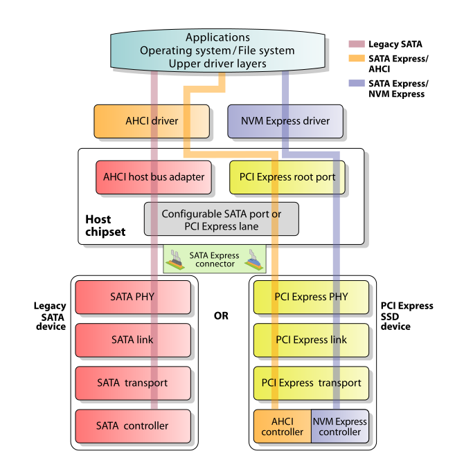
Often the mainboard’s silkscreen next to the M.2 slot will mention what technology an M.2 slot can accept. Checking the manual for the board in question is a good idea too. The reason for this confusion is that originally there was a Mini-SATA (mSATA) standard for SSDs which used the PCIe Mini Card form factor, which evolved into the M.2 form factor as well as the U.2 interface. The latter is more akin to the SATA and SAS interfaces, combining both SATA and PCIe channels into a single interface for connecting SSDs.
Meanwhile, the M.2 standard (after a brief detour with the short-lived SATA Express standard) was extended to support not only SATA, but also AHCI and NVMe. This is why M.2 slots are often (improperly) referred to as ‘NVMe slots’ when in reality NVMe is a PCIe-based protocol and defines no physical form factor or connector type.
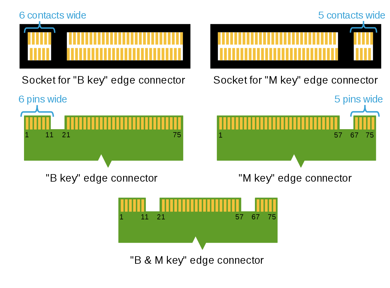
Meanwhile the M.2 form factor is by itself rather versatile, or convoluted depending on how you look at it. In terms of physical size it can have a width of 12, 16, 22 or 30 millimeters, while supporting lengths between 16 and 110 mm. On its edge connector interface a pattern of notches is used to indicate its functionality, which is matched on the M.2 slot itself. Most common are the ‘B’ and ‘M’ key ID notches in the Key ID list, which contains e.g.:
- A: 2x PCIe x1, USB 2.0, I2C and DP x4.
- B: PCIe x2, SATA, USB 2.0/3.0, audio, etc.
- E: 2x PCIe x1, USB 2.0, I2C, etc.
- M: PCIe x4, SATA and SMBus.
This means that the physical dimensions of an M.2 expansion card can be any of 32 different permutations, before the 12 possible Key ID notch permutations are included. Fortunately in mainstream use the industry appears to have standardized for storage cards on 22 mm wide connectors with any of a fairly limited number of lengths, resulting in NVMe SSD identifiers such as ‘2242’, which would be a 22 mm wide and 42 mm long card. Meanwhile SSD cards can be keyed for B, M or both.
Important to note here is that by now M.2 slots are commonly used as essentially PCIe expansion slots for situations where space matters. This is why WiFi cards are also commonly found in M.2 form factor.
Defining NVMe
This then lands us at the essential definition of what NVMe is: a standard interface for storage devices that are directly connected to PCIe. What makes NVMe so different from SATA is that the latter translates the PCIe protocol to the SATA protocol, which then has to be interpreted by a chip on the storage device that speaks SATA before any storage-related commands can be executed.
Instead, NVMe defines the interface which can be used directly by any operating system which has an NVMe driver. Commands are sent to the NVMe storage device, which in turn executes those commands to read or write data, or perform certain maintenance operations, like TRIM. As one can safely assume that any storage device that identifies itself as an NVMe device is a solid-state storage device (NAND Flash, 3D XPoint, etc.), this means that the NVMe protocol is designed around the assumption of a low-latency, high burst rate storage device.

Recently, a feature of NVMe called Host Memory Buffer (HMB) has become popular as a way to skip the need for a DRAM buffer on NAND Flash-based SSD. This feature uses part of the system RAM as a buffer, with relatively little loss in performance, with the buffer used primarily for an address mapping table cache.
As storage solutions keep evolving, new storage technologies such as 3D XPoint have made even such features already irrelevant in the long term, as 3D XPoint’s access speed is closer to that of a DRAM buffer than that of NAND Flash. As 3D XPoint SSDs do not have a DRAM buffer, the increased use of such SSDs may result in NVMe being optimized for such storage devices instead.
Hacking NVMe
At some point one has to wonder what you can actually do with NVMe, beyond buying NVMe SSDs and putting them into an M.2 B and/or M keyed slot on a mainboard. Here you should probably consider whether you’re more interested in hacking some solid-state storage together (if even just in the form of some DRAM or SRAM), or whether the M.2 slot itself is more intriguing.
Where full-sized PCIe slots are fairly big and the expansion cards offer a lot of space for big, clunky components like massive BGA chips and gigantic cooling solutions, M.2 expansion cards are intended to be small and compact, allowing them to fit in laptops. One could, say, combine an FPGA with the requisite SerDes and PCIe hardware blocks with an M.2 form factor PCB to create a compact PCIe expansion card for use in laptops and embedded applications.
Some recent hacks promise to add NVMe support to Raspberry Pi compute modules, replacing the SSD in a Pinebook Pro with a WiFi card, and reading out an iPhone’s NVMe Flash storage module using a ZIF adapter for PCIe.
Which is not to say that there is anything against someone trying to combine something as silly as making an NVMe storage drive using, say, core memory :)
Wrapping Up
Looking back on a few decades of computing, there has always been this distinction between system memory and storage, with the former being fast SRAM or DRAM volatile RAM. This distinction has decreased significantly in recent years. While NAND Flash-based storage along with NVMe means that we have the potential for extremely low latency and gigabytes per second of data transfer (especially with PCIe 4.0 NVMe), this is not the end of the story.
The newest thing appears to be the use of so-called ‘Persistent Memory’ DIMMs in regular system memory slots. These use Intel’s Optane solid-state storage, allowing for system RAM to be increased by up to 512 GB per module. Naturally, these modules currently only work in Intel (server) boards which work with these special memory modules. Their use is in buffering for example databases, where the large size would make an in-memory buffer prohibitively expensive or impractical (e.g. multiple TBs of DDR4 DIMMs).
By having what is essentially very fast, persistent storage directly on the CPU’s memory controller, latency is reduced to the absolute minimum. Even though 3D XPoint (as a form of Phase Change Memory) is as of yet not as fast as DDR SDRAM, it may show us a glimpse of what may lie beyond NVMe, with conceivably the difference between ‘system RAM’ and ‘storage’ completely obliterated or changed beyond recognition.


” Even though 3D XPoint (as a form of Phase Change Memory) is as of yet not as fast as DDR SDRAM, it may show us a glimpse of what may lie beyond NVMe, with conceivably the difference between ‘system RAM’ and ‘storage’ completely obliterated or changed beyond recognition.”
Security, where one is never certain something is gone even by the act of turning it off.
Though government surplus computers always seem to have their RAM pulled anyway. They’re either excessively paranoid, or it’s a hole already. Though you’d think even one round of one test in memtest86 would clear them… even if there is a practical way to read the exponentially decaying charge differences under liquid nitrogen from the last time it was used.
Where I worked RAM was pulled to keep it for other pc’s if somebody needs an upgrade. The ram is useable over many types and even generations of hardware…
This was also an issue with core memory, and magnetic media, nothing new here, this problem is 50 years old by now, maybe this is a new thing for you but the rest of us have been dealing with data destruction issues for decades now.
You missed the dark ages of consumer PC hard drives with MFM and RLL interfaces, but these were probably in use before many of your readers were born.
It was sort of covered. The common controller cards for those drives were integrated into the drives themselves. Those drives were IDE(integrated drive electronics). Those drives evolved into ATA. I am omitting some steps even then, it was sort of wild and woolly back then, but…
Actually IDE came after RLL and MFM IIRC as you used a card driver board often combined with floppy (on the 386 DX16 I had) controller etc.
And before then we had MFM controller cards and separate floppy controllers. …And serial cards (RS-232), and parallel cards, and video cards, and any other cards we needed, all separate. Might be why my PC-XT came with 8 expansion slots. I may have had as many as 6 slots populated at any one time with that old beast of a computer.
Yes, at that time the parallel interface consisted of about 11 74LSxx chips, the data output consisting of a real 8 bit register like 74LS574
There also was ESDI, sort of an in-between of MFM/RLL and IDE.
Anyway, they all spoke the WD1003 controller language.
And AT PCs (286 to early 486 gen) usually can’t differentiate between these.
With the exception of those server/workstation machines with built-in SCSI support in Setup/BIOS.
XT PCs usually had a dedicated MFM/RLL controller card for ST-506/ST-412 compatible HDDs.
The controller also had an on-board BIOS with a low-level routine that could be called via debug utility from DOS.
Anyway, these also were using the WD controller language. AT versions of these controllers sometimes came without the BIOS chip, thus.
By the way, IDE controllers weren’t really “controllers”, but host adapters / interface cards only.
They simply connected the IDE HDDs (AT Bus drives) to ISA bus.
Technically both were “st506” variants; that bus was like floppy controllers you were sending head positioning and stuff as analog on those wires iirc.
I’ll go you one better: somewhere in my piles i have one ESDI controller still, I think. https://en.wikipedia.org/wiki/Enhanced_Small_Disk_Interface
My high school computer club used to get retired TEMPST machines from the gov that we would strip and recycle. The nice ones would get setup for teachers to use. I remember the MFM connector and hard drives. We had a troubleshooting step called ‘the drop’ where we would pick the machine up and drop it from about 6 inches. Most of the time the system would boot after that.
Still useful today when laptops can’t find their SATA drive, i) determine orientation of drive inside machine (look for pics) ii) drop it 6″ onto the end or edge the connector connects from.
When SATA first started hitting the market, the company I was working for was having problems with SATA cables falling out, when the computers were being shipped. Eventually they resorted to hot-gluing them in.
The elephant in the room is that most consumer laptops have started dropping out extension ports: express card, SD slot, full-size USB, video connectors. RAM is more often soldered than not. The NVMe slot is here for now, but might follow a similar fate.
If I get the tone of the article right, the nVME should be able to act as a memory expansion. But so would Thunderbolt, in an ideal scenario. However, there are latency issues and bandwidth issues, so it will never be able to actually replace RAM, but just add more swap space.
Probably, future retro-computing will just add a USB-C module that does all the computing and rendering, while the laptop will just act as a dumb display and input. I just don’t see a way around this.
tl;dr: vote with your wallet and only buy hardware you can upgrade
Edit:
bad comment system put my comment NOT as reply
There are no options that I know of, speaking of ultrabooks. I bit the bullet for the first time, but I suspect it’s like with mobile phones and their headphone ports, chargers, headphones, SD slots, …
If a certain fruit company does something evil and people still buy in droves, the other manufacturers think people buy more because of that missing feature. Rant over.
You’re just looking at the wrong class of machine, it’s like going to the bicycle store and whining about them not having one with 4 wheels 4 seats and an engine.
That is my requirement and previous-gen machines had upgradable slots. It’s like going to the bicycle store and some customer coming in and telling you you should not be there.
Its like going to the bicycle store and being told that no-one makes a bike with a drink bottle holder, multiple gears and sprung front ends anymore because “no-one wants those features” (despite people comming into the bicycle store and asking for such a bike and despite previous bike models having such features)
No, it is like going to a car dealers, asking for a decent car with all the features your previous one had and instead getting offered only a bicycle, thou featuring glitter paint.
All are you are missing the point that you’re only offering the $88 of a basic walmart bike and you are going to get none of these features for that.
You want “what you used to get” okay I’ll tell you, for $1000 the first consumer laptops had mono screen, maybe a backlight, no hard disk, one floppy, serial port, parallel port. the end.
You’re all arguing “Why come if I buy the deluxe sports model for $70k it doesn’t come with the payload of the cheapest truck???”
If you buy the slim and light model it comes with as little as possible to make it the slimmest and lightest. Because that’s what that segment is about. You. are. buying. the. wrong. model.
With that analogy I can agree.
The thing is, they can still make bicycle with bottle holders, it’s just that the “biggest” bicycle maker got rid of them since they were costing 20c. I shouldn’t need to buy a car to get it.
Personally I don’t think we will see the line between memory and storage be all that muddled in the future.
Yes, 3D XPoint is a lot more responsive than Flash. But Flash isn’t all that impressive as is.
The typical hard drive has access latencies around 4ms on average. (7200 RPM and not taking into account any caches on the drive)
Flash can reach well bellow µs latency, but for very small arrays. This is expensive and mostly seen in Microcontrollers that execute directly from their Flash. “Enterprise grade” flash that optimizes at cost/GB will have far higher latency, in the few to tens of µs region.
3D Xpoint is a bit of a wash. I have seen quoted figures of sub 350ns write latency, but that is likely for a single cell, not an array. Optane modules from Intel on the other hand have typical latencies around 5-15µs, but this is from a “system” perspective, ie, protocol and controller overhead comes into play, as well as one’s software environment.
DRAM on the other hand has access latencies around 2-15ns at current.
The problem with latency is that it leads to our processor stalling due to not getting the data in time.
One can prefetch, but branches makes prefetching harder, since what side should you fetch?
Branch prediction partly solves this issue. But from a performance standpoint, we should fetch both sides. But if we have more latency, we need to prefetch even earlier, risking more branches. In other words, peak bandwidth required by our processor increases at an exponential rate compared to latency. A rate that is application dependent as well.
Caching might seem like the trivial solution to the issue, but the efficiency of cache is proportional to the latency. To a degree, cache is a magic bullet that just makes memory latency disappear. But every time an application calls for something that isn’t in cache, then the application stalls, as long as there is threads to take its place that also have data to work on, then you won’t have a performance deficit other than thread switching penelties, but if you don’t have such threads, then the CPU stalls.
One can ensure that more threads have their data by just making the cache bigger, but cache is a lot more expensive than DRAM.
In the end, it all leads to the fact that increasing latency will require an arbitrary amount more cache for a similar system performance.
Going from the few ns latency of DRAM to the couple of µs latency of current persistent memory is not realistic as an actual replacement for DRAM, even if it reduces its latency to a 100th it is still not impressive as far as memory goes.
Though, the use of persistent DIMMs for storage caching or as a “RAM drive” of sorts still has major advantages, but for program execution it is laughable.
And I don’t suspect this to change any time soon.
But I can see a future where the main memory relocates into the CPU. (mainly for mobile and consumer platforms)
Where the CPU itself has an HBM memory chip or four on it supplying relatively low latency and high bandwidth memory to the CPU, while the external buses are used for IO and storage. But this isn’t all that realistic in more professional applications, since some workstation applications honestly needs 10’s-100’s of GB of actual RAM to get good performance.
The Optane latencies you are quoting come from NVDIMMs which are effectively DDR4 modules with a slightly modified protocol/inferace to 3dXpoint.
The several uSec latencies of NVMe is due to the controller layout (optimized for $ & density) and PCIe latency limitations… when you put 3dXpoint on an NVDIMM the latency goes way down.
350ns is still huge as far as RAM memory goes.
Considering how there is noticeable performance difference between different DRAM latencies even if they have the same bus clock speed. Though, considering how DRAM has the main limitation that it can’t really use the bus while waiting on the module, then this isn’t the most fair comparison.
Indeed, if you’re willing to consider 350ns as acceptable, you may as well build yourself a bank of conventional EEPROMs
350ns is good enough for really low latency storage.
But considering the access time of even the “slow” DRAM chips in the 80’s were an order of a magnitude faster, then it sure isn’t impressive as far as execution is concerned.
I don’t think persistent dimms will actually replace RAM, only complement it in some workloads where a large scratch disk with very high bandwidth is needed, or database caching, since that is the big strong side of a memory channel. Having 20+ GB/s of bandwidth right there is a nice feature.
150ns to 120ns is what I’ve seen in PC/XT class, 256kB and 1MB SIMMs you might find 120 or 100ns versions of those, used in the first 286es to use SIMMs but not much good beyond that. When speeds got over 10Mhz, then 80ns became bare minimum.
Though, in the PC/XT days, cache weren’t as much of a thing.
It did exist in larger computing systems though. (Like larger mainframes.)
Cache needs to reach a certain since size before it will actually start doing anything of note. The biggest performance boost from cache is when the shorter loops within an application can retain their code in cache, but then one needs enough of it for that code. + all other stuff that also resides in cache, like data for the next thread waiting to run. (otherwise the next thread will instantly stall.)
So 80ns RAM were needed on the 10MHz processors of the day because it literally couldn’t do much better then to fetch the data only a couple of cycles before it needed the data. Stalling were the name of the game if the processor were faced with a branch. (Branch prediction were a thing, so didn’t actually stall that often.)
When cache comes in, one can start working with memory that is slower than the core clock of the processor, but only to a degree. Because cache can only limit a core’s apatite for memory bandwidth proportionally to how much cache we have and what the application is working on.
And fixing latency is something cache can’t even do. If the data isn’t cached, it simply isn’t cached, then one needs to go and fetch it. (Fun fact, adding cache to a system usually increases memory latency within the system, since the memory controller will always have to check cache first. If the data is on the chip, then it is a waste of precious memory bandwidth to leave the chip to get that data. (unless there is coherency reasons behind it, though this is only the case in multi socket systems, or if dealing with a co processor like a GPU, network/storage controller, etc.))
And if we have a particularly memory heavy workload that the application skitters about within like a maniac, then cache won’t really help much, unless it is large enough to handle that whole dataset. Here the memory latency of the system will be one of the main performance limits to such an application. (Unless the application can be done in parallel, then we will instead have to consider Amdahl’s law for both the application and dataset.)
Sadly a fair few applications falls into the category of being fairly sporadic in what they want to work with next.
Meaning that latency does play a noticeable role in system performance as far as memory is concerned. Largely regardless of how much cache the system has. (within practical limits that is. If cache is large enough for half the dataset, then it will practically save in on the latency half the time. Though, for a many GB large dataset, the cache would be awfully slow in itself due to its size alone, ie one is shooting oneself in the foot at that point…. Not to mention a dataset that is 100’s of GB)
Someone correct me if I’m wrong, but I thought 350ns was the time to the first access, then further accesses in the same column (row?) went a lot faster. There was a blurb, possibly in The Next Platform, about running an ML job on encrypted data and using the Optane DIMMs as extra RAM. The writeup said it worked well.
And indeed, here it is: https://www.nextplatform.com/2020/12/08/boosting-memory-capacity-and-performance-while-saving-megawatts/
Sounds like they hooked some shared library calls to play with which type of dimm was used for which objects.
Indeed. As the other commenters stated, it’s really slow. 1970s era EPROMs had roughly 250ns access time already, if memory serves. While the SIMM modules, 4x 1MiB, of my 286-12 PC had 60/70ns access time. That being said, the technology comes close that. In a few years, maybe, it will surely catch up with access time of 1980s RAM.
You are confusing it with not being able to read while writing to FLASH memory.
SDRAM/DDR have multiple internal memory banks. You can access one while the other one is busy.
True, forgot about that part.
Let’s not forget the current security issues that plague all kinds of DMA. That’s why I doubt external memory extensions will be feasible in the near future, since it gives access to a bad actor to all the data going through the CPU. We would need a different paradigm to deal with that.
Having one coherent memory space have its pros and cons.
It eases up development, but can also be a security detriment.
Though, it also depends on how one’s memory policy works, especially on an architectural level since it is there that the software can’t do much about it.
The problem with a lot of hardware security flaws is that hardware makers don’t really provide much actual tools for security, but rather tries to over engineer a system that can do it on the fly for the software. With limited success. Now, a lot of architectures do have tools for setting up memory restrictions, but the restrictions aren’t always all that practical.
These day though, modern CPUs have different levels of cache. The one I’m using right now (3700X) has 512KB of L1 cache (as much as the entire memory of my first computer!), 4MB of L2, and 32MB(!) of L3. After missing on all of these, then the CPU will check main memory.
As far as I understand it, the aim of Optane (and similar) is not to replace RAM, but instead to fit at a level between RAM and the storage. In much the same way as SSDs are sometimes used to cache data from spinny hard drives.
Persistent DIMMs can either be used as storage, caching for storage, or as “memory”.
Where the “memory” part makes its largely indistinguishable from other RAM, other than its far greater access latency.
The existence of multiple cache levels is true, but that were already considered in my comment.
The number of cache levels and how their are configured has little impact on the core limitations of caching in general when taking regards to memory latency in a larger system.
If the cache system as a whole doesn’t have the content, then the application will stall for a time that is proportional to the access time of the memory. One can switch thread here, and processors typically does. But thread switching requires that the new thread has content to work on, and thread switching tends to have a performance penalty in itself.
But, in a typical 3 layer cache system the processor core would already be stalling by the time we get to L3. Since L1 is used for taking the grunt work, L2 is for just in time delivery before the core stalls, and L3 is “We don’t leave the chip if the data is in cache!” since that would be a waste of memory bus bandwidth otherwise. But non of this really matters since one doesn’t stall for all that many cycles if the content were in L3. And with both out of order execution and SMT these few cycles matters even less.
Also, the “512KB of L1 cache” is actually smaller in practice, I will take a “wild” guess that you have a quad core CPU, not because they are really common, but rather that an x86 core has two L1 caches that are practically always 64KB each for quite some time now. (unless one has a more modern AMD processor, they have some odd 96KB for each L1 last I checked. It really don’t matter much, and it is usually better spend more on L2. But I guess that you don’t have 2.66 cores.) The reason I say it is “actually smaller” is because each core has its own set of L1 caches, it can’t make any use of the L1 cache in another core, so even if the content in is “L1” a given core can still have to stumble all the way to L3 to get it.
Persistent DIMMs on the Intel platform can also use one’s regular DRAM as a 4th layer of cache.
For some computing applications, using Optane as memory would work fine, for others it would be abhorrent.
For storage caching and scratch disk applications, it is already a proven solution that kind of just continues on from where Flash already were.
You mentioned persistent memory DIMMs as a function of Optane memory modules. There is a more pedestrian variant that is cheaper: NVDIMMs. These contain RAM and conventional NAND flash. When the system powers down they copy the RAM to flash, many have a power outage capability too, so even if they are not shutdown properly they can scram the memory to flash before they run out of juice.
NVNE Drives Form-Factor was a bad decision. If they the form-factor them a little wider, we wouldn’t have to choose between storage with the QLC drives, and the reliability of traditional flash chips.
As a content creator, about 20% of my SSD is endurance has been used up.
Non-volatile RAM has been around in microcontroller sizes for awhile. See the MSP430FR[…] chips, and you can get it in SOIC-8 footprints as well. It’s called FRAM or FeRAM (ferroelectric) in those affordable low-density chips.
It has not been available in high-density/GHz-speed formats, but it was still fast compared to an MCU’s SRAM, and personally I always had trouble finding a use-case. Fast boots, sure. And it’s nice for storing config data, but config data is usually not written to very often.
I dunno, I think it’s very cool. Maybe in the future we’ll be able to live without volatile memories, and that would be something. But I don’t see it changing my life in the near-term.
Now Simtek had some interesting stuff, “AutoStorePlus™ nvSRAM QuantumTrap™ CMOS Nonvolatile Static RAM” which was a fastish for the time SRAM which on power off would dump data into a “quantum trap” using the charge in a capacitor, and reload it at power on. Claimed data retention was 100+ years
I don’t know if it’s gone anywhere since Cypress bought them, or got renamed, or suffered the “not invented here” problem.
I have just the one device, on an old Compaq enterprise storage card, that may get picked off to play with, as soon as I can figure out a way to use a whole 8096 bytes in one go.
Things will get blurrier ( i wasn’t sure that was even a word ). With PCI gen 5 and CXL there will be coherence between ‘main’ memory and PCI items – accelerators, storage,,,, or memory.
“One could, say, combine an FPGA with the requisite SerDes and PCIe hardware blocks with an M.2 form factor PCB to create a compact PCIe expansion card for use in laptops and embedded applications.”
Already exists, for surprisingly cheap, as the SQRL Acorn. Good luck fitting it into most laptops with the tall heatsink, but it will do just fine on a mini ITX or other SFF motherboard if you want a compact compute module.
primary storage is directly addressable by the CPU’s most primitive instructions. secondary storage is not. It is usually slower out of practicality but there is not reason it must be that way, and plenty of embedded systems have had SRAM secondary storage on a bus no slower than the primary memory bus.
The distinction does alter how software and operating systems should handle the two different worlds of memory. Swapping and multiple layers of cache does blur the lines for software at least in the higher layers. There are still considerations found at potentially any layer of software in terms of what constitutes an atomic memory operation.
tl;dr: vote with your wallet and only buy hardware you can upgrade
Xpoint did that years ago. I postulated then that cpus should attach to that without separate memory and storage. Maybe we’ll get there one day.
In principle you could do that now. In practice I wonder if (U)EFI or BIOS could cope with it, but that’s just a Simple Matter Of Programming. You’d want to be sure almost off your code would fit in the CPU caches as measured by time spent in that code, not simply bytes. It would be fine to have a 200 megabyte executable as long as it spent 99.99% of it’s time in one small, tight loop.
It’s all about sizing (and, yes, organizing) the caches. Fun fact – the IBM Blue Gene L has 8 Kbyte instruction and data caches because a code called Quantum Chromodynamics (“QCD”) basically stays in one very tight loop most of the time. IBM had one particular customer in mind. In fact, the machine was originally called QCDOC – “QCD on a Chip”.
If you were ahead of the game you were booting or paging off mini PPCIe in the early two thousands….
Got a ~13 year old Toshiba Satellite C2D, has that Intel Turbo memory in it, 1GB of drive cache. It was an option on Thinkpad T400s as well, which I also have one of, that’s in generally better shape takes more RAM etc, so pondering robbing the Satellite and sticking it in that…. although really I should not bother and just use SSD. Also haven’t been inside the T400 deep enough to know if it’s actually got the socket mounted, might find bare pads and a ton of passives missing. There’s also a lot of “Yeah we kinda wanted a mini PCIe slot but we were just gonna stick a 56k modem in it, or a 3G card, or BT, or GPS, so didn’t bother with full implementation that would make it useful for storage or any other high performance use.” so what works is what it shipped with and good freaking luck making anything else work in there.