Now that it is relatively cheap and easy to create a PCB, it is a common occurrence for them to be used in projects. However, there are a lot of subtleties to creating high-performance boards that don’t show up so much on your 555 LED blinker. [Robert Feranec] is well-versed in board layout and he recently highlighted an animation on signal crosstalk with [Eric Bogatin] from Teledyne LeCroy. If you want a good understanding of crosstalk and how to combat it, you’ll want to see [Eric’s] presentation in the video below.
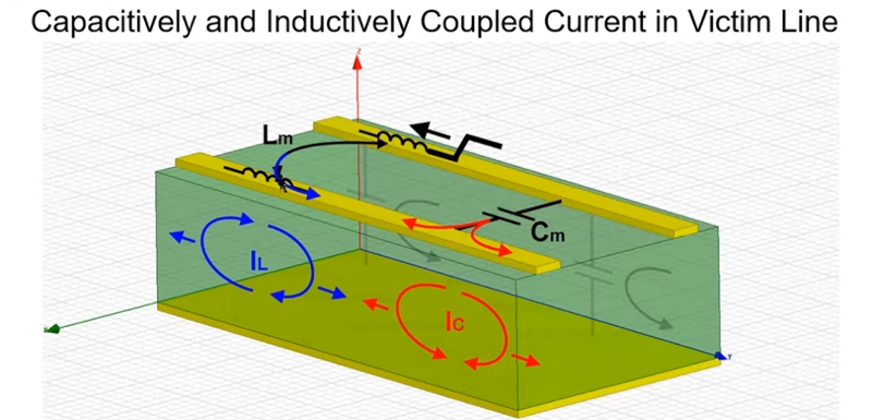
Simplifying matters, the heart of the problem lies in running traces close together so that the magnetic fields from one intersect the other. The math is hairy, but [Eric] talks about simple ways to model the system which may not be exact, but will be close enough for practical designs.
The models use inductors and capacitance to represent different modes of crosstalk, and it’s likely you already know how to deal with those quantities. The video shows some simulations and also suggests methods to control the problem.
Even though the topic is PC boards, some of the same ideas apply to cables. Ethernet cables, for example, have specifications for FEXT for similar reasons.
Our own [Bil Herd] has a take on similar topics you might enjoy. [Feranec] is behind Fedevel Academy which we’ve read reviews about before.


“Now that it is relatively cheap and easy to create a PCB”
Is it though? Or have enough people started building projects that are so tiny that there is a market now for PCBs which are cheap only because they are so small?
Don’t get me wrong, with tiny smd parts you can do some awesome things so long as your project is all small signals and doesn’t need too many connection offboard. I’m working on a project that has a lot of connectors and they can only be miniaturized so far because they carry current. Something that seemed so simple is starting to look expensive because all those connectors take more PCB real-estate and the price goes up with size quickly!
I’m starting to think I might need to etch it myself and I really don’t like doing that.
It’s almost as if the cost of manufacturing scales with complexity and material used.
I treat my PCB like downtown Tokyo real estate. I have pushed the PCB to their design rules. I don’t waste space on useless art, logos, odd shapes as I pay dearly on the square inch footage. I have more sense than vanity.
Looking at some of my boards stats, the parts typically take up 75% of PCB surface. I etch my PCB if they are very loose specs or cost a lot.
You can consider producing small 4/6/whatever layers “boardlet” modules sitting on a large 2-layer cheap motherboard.
Services like JLCPCB are making it incredibly cheap. A few weeks ago, I ordered 5 PCBs, about 250x100mm so not small, for about £9 plus shipping.
I learned this the hard way back in the early 80s – I had a PCB layout that had a reset line between the ground trace and the 8 data bus lines – every time 5 or more of the data lines went from high to low at the same time, the coupling onto the reset line would pulse it low and reset the system – it drove me crazy for the better part of a day until I figured out what was happening.
This makes me understand the problems I had with a certain pcb some years ago. Great article.
The layout world can still be wonderfully black-art analog ;~) When I was making a very early smart audio card for the ISA bus, using a TMS320C30, some SRAM and other goodies, to keep the cost reasonable, I managed full speed using only a double-sided board by using the address lines on one side running mostly orthogonal to the data lines on the other si,de. Since address was driven and stable while data was changing…the address lines worked as a ground plane for the data lines. Worked great and looked cool besides.
Would reducing the trace width help in any way (assuming the traces stay at the same position so that the separation increases)?
You want to provide a better return path for the signals so that they don’t use each other for so (i.e. crosstalk hapens)
– The most effective way to reduce crosstalks is to use a multlayer PCB with signal/ground layers
– Failing that, a ground layer *and* reduce the thickness of the FR4. Thinner PCB without ground plane won’t help.
Making tract thinner still doesn’t give the signals a return path, so it might reduce the symptom, but not solve the underlining cause. It’ll also make the traces more inductive (higher impedance), so expect more overshoots and undershoots.
You might be able to space them to give more space around the most critical signals and shifting the crosstalks to the non-critical ones. e.g. your clocks, data strobe lines
If possible, reduce the slew rate of the signals. i.e. use the slowest drivers that would run.
your clocks, data strobe lines : critical signals as they are used for data transfers. Other signal can have crosstalks s long as they are stable during the setup and holdtime.
When working with fast stuff…almost everything these days, you generally set track width such that you impedance match the signal to prevent reflections and ringing. Thickness, dielectric constant, ground plane all are taken into account to achieve this.
Of course, there are setups that deliberately mismatch and use the reflection to advantage…like the PCI bus.
Ringing, overshoots, undershoots can radiate and cause EMI as the excess energy got to go somewhere. Use of series termination for impedance matching can help a lot. Even if it isn’t a perfect match, the resistor is lossy and it can help to damp out and dissipate the ringing.
These days, we have slew rate control on FPGA, CPLD and even microcontrollers – even my $0.20 part have it.