PCI Express (PCIe) has been around since 2003, and in that time it has managed to become the primary data interconnect for not only expansion cards, but also high-speed external devices. What also makes PCIe interesting is that it replaces the widespread use of parallel buses with serial links. Instead of having a bus with a common medium (traces) to which multiple devices connect, PCIe uses a root complex that directly connects to PCIe end points.
This is similar to how Ethernet originally used a bus configuration, with a common backbone (coax cable), but modern Ethernet (starting in the 90s) moved to a point-to-point configuration, assisted by switches to allow for dynamic switching between which points (devices) are connected. PCIe also offers the ability to add switches which allows more than one PCIe end point (a device or part of a device) to share a PCIe link (called a ‘lane’).
This change from a parallel bus to serial links simplifies the topology a lot compared to ISA or PCI where communication time had to be shared with other PCI devices on the bus and only half-duplex operation was possible. The ability to bundle multiple lanes to provide less or more bandwidth to specific ports or devices has meant that there was no need for a specialized graphics card slot, using e.g. an x16 PCIe slot with 16 lanes. It does however mean we’re using serial links that run at many GHz and must be implemented as differential pairs to protect signal integrity.
This all may seem a bit beyond the means of the average hobbyist, but there are still ways to have fun with PCIe hacking even if they do not involve breadboarding 7400-logic chips and debugging with a 100 MHz budget oscilloscope, like with ISA buses.
High Clocks Demand Differential Pairs
PCIe version 1.0 increases the maximum transfer rate when compared to 32-bit PCI from 133 MB/s to 250 MB/s. This is roughly the same as a PCI-X 64-bit connection (at 133 MHz) if four lanes are used (~1,064 MB/s). Here the PCIe lanes are clocked at 2.5 GHz, with differential signaling send/receive pairs within each lane for full-duplex operation.
Today, PCIe 4 is slowly becoming adopted as more and more systems are upgraded. This version of the standard runs at 16 GHz, and the already released PCIe version 5 is clocked at 32 GHz. Although this means a lot of bandwidth (>31 GB/s for an x16 PCIe 4 link), it comes with the cost of generating these rapid transitions, keeping these data links full, and keeping the data intact for more than a few millimeters. That requires a few interesting technologies, primarily differential signaling and SerDes.
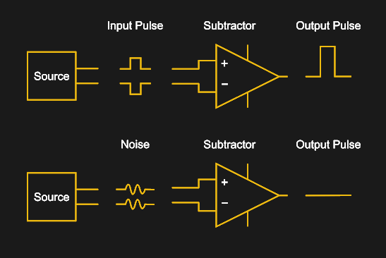
Differential signaling is commonly used in many communication protocols, including RS-422, IEA-485, Ethernet (via twisted-pair wiring), DisplayPort, HDMI and USB, as well as on PCBs, where the connection between the Ethernet PHY and magnetics is implemented as differential pairs. Each side of the pair conducts the same signal, just with one side having the inverted signal. Both sides have the same impedance, and are affected similarly by (electromagnetic) noise in the environment. As a result, when the receiver flips the inverted signal back and merges the two signals, noise in the signal will become inverted on one side (negative amplitude) and thus cancel out the noise on the non-inverted side.
The move towards lower signal voltages (in the form of LVDS) in these protocols and the increasing clock speeds makes the use of differential pairs essential. Fortunately they are not extremely hard to implement on, say, a custom PCB design. The hard work of ensuring that the traces in a differential pair have the same length is made easier by common EDA tools (including KiCad, Autodesk Eagle, and Altium) that provide functionality for making the routing of differential pairs a semi-automated affair.
Having It Both Ways: SerDes
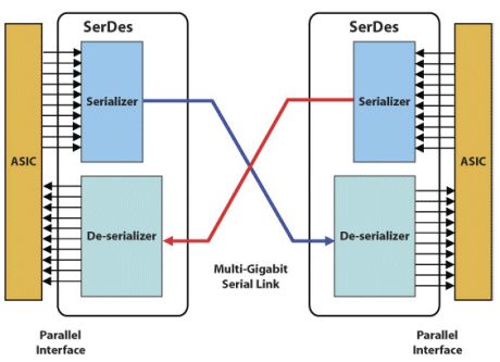
A Serializer/Deserializer (SerDes) is a functional block that is used to convert between serial data and parallel interfaces. Inside an FPGA or communications ASIC the data is usually transferred on a parallel interface, with the parallel data being passed into the SerDes block, where it is serialized for transmission or vice-versa. The PCIe PMA (physical media attachment) layer is the part of the protocol’s physical layer where SerDes in PCIe is located. The exact SerDes implementation differs per ASIC vendor, but their basic functionality is generally the same.
When it comes to producing your own PCIe hardware, an easy way to get started is to use an FPGA with SerDes blocks. One still needs to load the FPGA with a design that includes the actual PCIe data link and transaction layers, but these are often available for free, such as with Xilinx FPGAs.
PCIe HDL Cores
Recent Xilinx FPGAs not only integrate SerDes and PCIe end-point features, but Xilinx also provides free-as-in-beer PCIe IP blocks (limited to x8 at PCIe v2.1) for use with these hardware features that (based on the license) can be used commercially. If one wishes for a slightly less proprietary solution, there are Open Source PCIe cores available as well, such as this PCIe Mini project that was tested on a Spartan 6 FPGA on real hardware and provides a PCIe-to-Wishbone bridge, along with its successor project, which targets Kintex Ultrascale+ FPGAs.
On the other sides of the fence, the Intel (formerly Altera) IP page seems to strongly hint at giving their salesperson a call for a personalized quote. Similarly, Lattice has their sales people standing by to take your call for their amazing PCIe IP blocks. Here one can definitely see the issue with a protocol like PCIe: unlike ISA or PCI devices which could be cobbled together with a handful of 74xx logic chips and the occasional microcontroller or CPLD, PCIe requires fairly specialized hardware.
Even if one buys the physical hardware (e.g. FPGA), use of the SerDes hardware blocks with PCIe functionality may still require a purchase or continuous license (e.g. for the toolchain) depending on the chosen solution. At the moment it seems that Xilinx FPGAs are the ‘go-to’ solution here, but this may change in the future.
Also of note here is that the PCIe protocol itself is officially available to members of PCI-SIG. This complicates an already massive undertaking if one wanted to implement the gargantuan PCIe specification from scratch, and makes it even more admirable that there are Open Source HDL cores at all for PCIe.
Putting it Together
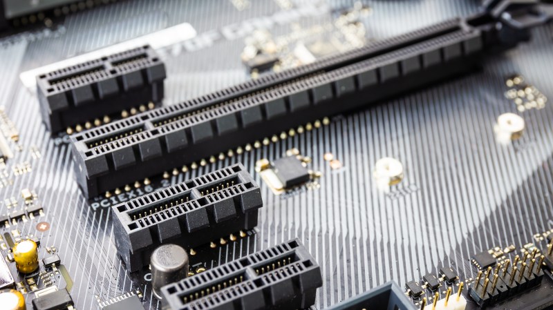
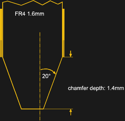
The basic board design for a PCIe PCB is highly reminiscent of that of PCI cards. Both use an edge connector with a similar layout. PCIe edge connectors are 1.6 mm thick, use a 1.0 mm pitch (compared to 1.27 mm for PCI), a 1.4 mm spacing between the contact fingers and the same 20° chamfer angle as PCI edge connectors. A connector has at least 36 pins, but can have 164 pins in an x16 slot configuration.
An important distinction with PCIe is that there is no fixed length of the edge connector, as with ISA, PCI and similar interfaces. Those have a length that’s defined by the width of the bus. In the case of PCIe, there is no bus, so instead we get the ‘core’ connector pin-out with a single lane (x1 connector). To this single lane additional ‘blocks’ can be added, each adding another lane that gets bonded so that the bandwidth of all connected lanes can be used by a single device.
In addition to regular PCIe cards, one can also pick from a range of different PCIe devices, such as Mini-PCIe. Whatever form factor one chooses, the basic circuitry does not change.
This raises the interesting question of what kind of speeds your PCIe device will require. On one hand more bandwidth is nice, on the other hand it also requires more SerDes channels, and not all PCIe slots allow for every card to be installed. While any card of any configuration (x1, x4, x8 or x16) will fit and work in an x16 slot (mechanical), smaller slots may not physically allow a larger card to fit. Some connectors have an ‘open-ended’ configuration, where you can fit for example an x16 card into an x1 slot if so inclined. Other connectors can be ‘modded’ to allow such larger cards to fit unless warranty is a concern.
The flexibility of PCIe means that the bandwidth scales along with the number of bonded lanes as well as the PCIe protocol version. This allows for graceful degradation, where if, say, a PCIe 3.0 card is inserted into a slot that is capable of only PCIe 1.0, the card will still be recognized and work. The available bandwidth will be severely reduced, which may be an issue for the card in question. The same is true with available PCIe lanes, bringing to mind the story of cryptocoin miners who split up x16 PCIe slots into 16 x1 slots, so that they could run an equal number of GPUs or specialized cryptocoin mining cards.
It’s Full of PCIe
This flexibility of PCIe has also led to PCIe lanes being routed out to strange and wonderful new places. Specifications like Intel’s Thunderbolt (now USB 4) include room for multiple lanes of PCIe 3.0, which enables fast external storage solutions as well as external video cards that work as well as internal ones.
Solid-state storage has moved over from the SATA protocol to NVMe, which essentially defines a storage device that is directly attached to the PCIe controller. This change has allowed NVMe storage devices to be installed or even directly integrated on the main logic board.
Clearly PCIe is the thing to look out for these days. We have even seen that System-on-Chips (SoCs), such as those found on Raspberry Pi 4 boards now come with a single PCIe lane that has already been hacked to expand those boards in ways thought inconceivable. As PCIe becomes more pervasive, this seems like a good time to become more acquainted with it.


You can get non name drives that mount into a mpcie socket and you can get sata drives that mount into m2 sockets. So using the form factor as its main benefit is like saying the only thing the Romans gave us was wine
What have the Romans ever done for us?
Speaking of open ended 1x slots, I once had a mini-ITX system that needed better graphics than the onboard IGP, but only had a closed 1x slot. There were parts in the way on the board as well, so converting it to open ended wasn’t an option. So, out came the bright flashlight to make sure there weren’t any traces under the extra (beyond 1x) part of the connector and then came the rotary cutter. It was pretty fun to cut into a GPU and wonder if I was destroying it or making it more useful (It was a many year old cheap Nvidia G210).
Once I had cleaned off the dust, I put it in the target and it didn’t work. :( Searching around, I found out that there’s a presence detect pin on the 1x part of the card (and on the 4x, 8x, and 16x, IIRC). Being a native 16x card, the 1x presence wasn’t asserted. So, I put a little bodge wire in the socket of the MB and reinserted the card. It worked! I later soldered the bodge to the card itself to make it more portable to different MB’s in case that was ever needed.
Maya, do you know much about the presence detect and how that works with >1x cards in an open ended 1x slot? I’m curious if the card has to be prepared for that as well or does the slot do something special? Thanks for the great article!
Oh, please do a follup on how bifurcation works! I’m very curious and I don’t know enough to know where to start looking. I keep seeing these dual N.2 4x slot to 8x host adapter cards and they all are passive and realy on the host to support bifurcation. How does one even know if that’s an option?
That fully depends on the switch / root complex that offers these lanes. It needs to be able to assign subsets of lanes to different endpoints, and some (usually, server-style hardware) can, others simply can’t. And as far as I can guess transceiver architecture, the consequences of support are quite far-reaching, so it’s nothing a firmware update could add.
Reminder – there are no more northbridge chipsets in computers. PCIE is inside the CPU, meaning if it works in some motherboards it has the potential of working everywhere, its all a matter of firmware after all. That is unless AMD comes along and tells you x470 “chipset” doesnt get the PCIE 4 because “reasons”, or PCI Express Resizable BAR support once again linked to x570 while its CPU internal matter. We are living in a soft-lock era of computing.
no, whether or not your root complex (and reminder, there’s plenty of mainboards with PCIe switches outside your CPU) supports bifurcation is not only a firmware update away. Can’t add a second set of high-speed control registers via software.
I’d love a good article on bifurcation. From my research, it’s indeed supported on some sexy motherboards like the ASRock ROMED8, but the devil is in splitting the clock signal to each device. This requires some active components.
I’d love to be able to buy a 16x-to-4x4x riser cable, but none are available. I contacted a manufacturer once, and their answer was just, “show us a working cable and we’ll clone it.” Alas.
There are recently developed NVMe cards for up to 4 devices each. From what I understand of your question, this is nearly exactly what you are looking for?
PCIE bifurcation was a thing back in Core2 and first i-core days, with eGPU PE4C V2 supporting PCIe x2 allowing you to recombine split PCIE links from inside the laptop (one pciexpress + one mpcie). Apparently Intel dropped support for it in Sandy Bridge and later CPUs. It requires @Nando4 eGPUSetup to reprogram PCIE controller.
buuut, these will work only with the BIOS intended for them…
riser.maxcloudon.com has some cable based one, i was running 4 gpus on one 16x slot on a threadripper motherboard
Well I don’t want to get lost all night on “oooh shiny!” rabbitrails by finding one for you, but I’m fairly sure I’ve seen them on AliExpress.
PCIe 4 has enough problems working on a PCB as is and you *want* extra cable length + connector insertion losses on top of the high frequency losses. One would need to have repeaters to compensate for hgh frequency losses.
While it is possible that some PCIe4 riser would/could work with some combinations of motherboards and/or GPU, they are a kludge beyond the PCIe 4 specs.
I loved your story, thank you!
If you don’t want to void your motherboard warranty there are adapters out there that allow you to plug a 16 lane card into an 8 lane slot. The card sticks up and you might have trouble with the connectors but it works great if you can get it to fit.
In that case you might be better off getting a pcie riser cable and mounting the card elsewhere. There are cases now that have a 2x wide card slot for house sideways above the normal expansion slots and often come with the riser cable to facilitate it’s use. It’s a nifty idea. For anyone thinking of using such a device, be aware that cheaper really does mean worse for pcie extenders, check reviews and buy the best one your budget allows. The cheaper you go the more likely their will be signal degradation.
I made an ISA bus card with a CPU (8051), memory (double buffering), and D/A converters once (for driving laser scanners). Worked great, took me a few weeks to design. It was a full-size ISA card, with a daughterboard on top of it, containing the analog D/A parts.
I remember that interfacing the card to the ISA bus was just a few 74LS244’s, a 74ls139 and a 74LS30 for address decoding, and I think that was about it.
If I would have to make that same card now, I would probably go for PCIe. For one, PCI is not easy to interface either (well, ok, you can buy one-chip PCI controllers these days), so why not go the whole way immediately? And that almost certainly means choosing for an FPGA.
So my card would now be a half-size card with an FPGA and the analog D/A part (need precise D/A converters). Put the PCIe controller in the FPGA, put a CPU in the FPGA, memory is already in there (surely there is 2 x 32KB in there).
For sure, the design will be hundreds of times more complex than my ISA card. But I wouldn’t notice it, because I just drag some stuff into my FPGA and bind it all together with a few lines of glue logic. I would still have to write the software for the CPU, though. :)
Standing on the shoulders of giants. :)
Why not use USB? It’s easy, well documented and plenty of bandwidth.
Because signed drivers are a pain in the a$$. (if you are stuck supporting Windoze) I am never makin another embedded USB device. Ethernet is cheap, easy, and pretty damn fast.
Looks like with a bit of care, you can sidestep most of the driver signing issues in Windows these days: https://stackoverflow.com/questions/42831608/how-to-install-winusb-driver-through-customized-inf-file-on-windows-10 (as a bonus, WinUSB doesn’t require kernel level programming and, when used via libusb, can even offer cross platform compatibility)
Make it look like a serial port or an ethernet dongle or a keyboard or whatever and you won’t need a driver.
They’re really not.
most PCs nowadays still come only with 1Gb ethernet…USB3.0 has 5Gb bandwith and a modern PC has several of them…
> Ethernet is cheap, easy, and pretty damn fast.
Plus it’s near realtime which sometimes is a lot more important than being the fastest, tolerates long cables, electrically insulated out of the box, and protocols are 100% open and stackable: from talking to the next chip to another continent it’s just a matter of layering completely open and highly tested protocols.
PCI is easy and doable with a small CPLD, or even two GAL chips if you are crazy enough (cheapest POST cards).
PCI yes, but PCIe is non-trivial. Unless you use a PCIe to something-else chip of course (usb, serial, ethernet, …)
PCIe connectors make for a low cost high speed interboard connector with or without PCIe.
But don’t forget the cards still need mechanical support or they will fall out. The pins also have a nasty habit of bridging at the bend where it is impossible to inspect, then the spacing between sockets makes it difficult to rework without melting the socket next to it. Then you have the extra back and forth with the pcb supplier over the card edge connector as to whether you need a prototype with normal plating and no chamfer, or double the cost to get gold fingers and proper chamfer. Personally I wont be using them again.
It’s worth noting that routing a PCIe lane “bundle” is significantly easier than routing legacy PCI.
Sure, the clock speed is high, but:
If you combine multiple lanes, you don’t have to match length between lanes – the lane itself should be length-matched.
Don’t overdo it. Seriously. People put faaaar too much though into length matching. A single cm of difference on “usual” PCBs is 10⁻² m/ (2·10⁸ m/s) = 5·10⁻¹¹ s in difference. If you tolerate 5% of a clock cycle in difference, you can still use that “mismatched lane” for clocks up to 10 GHz.
“Differential signaling” is important. It seriously is, because it’s where robustness comes from. “differential pair routing” is … nice to have, since it inherently solves 1./2., and it slightly improves cross-talk, but seriously, in any sensible PCB stackup, coupling between the ground plane below and each conductor of the differential pair is orders larger than between the two pairs. That follows from the geometry of conductor and plane being parallel plates with a large area and 100% higher-epsilong dielectric, whereas conducturs between them are not only further apart (averaged over the width of the conductor), but also adjacent on the “shorter side”, i.e. that model plate capacitor is 35 µm high, seriously.
Especially the first point however massively simplifies all layout. You need to add a through-hole thing somewhere in your PCI bus? Uff, get ready to just scramble to fit the massive amount of lines around an obstacle. You need to make a slot in your PCB that spans 90% of its width? Well, with PCIe you can route half of the lanes on the west side, half on the other, with a 20cm detour, and typically nothing will mind.
So, are you saying that if I have an 4-lane device, lane A can be (for example) 10CM long, and lane B be 20CM long, lane C be 30cm long, and (for giggles) lane D be 40CM long and the SERDES inside of the PCI controllers will re-align the data? I get that the difpair A,A! need to be pretty close in length, but how forgiving are the mismatches in lane-lengths for 4X, 8X and 16X
There is specs for how much length difference one can have between lanes in the PCIe spec.
But I don’t know them off hand.
But to a degree, “yes”, one can just stich it back afterwards. One just adjusts the length of a small FIFO buffer for each lane. As long as the difference is within the capabilities of the FIFOs, then it isn’t a problem. Now, I don’t know if PCIe uses length selectable FIFOs, but it would be a trivial implementation to have.
But a casual 16 stage FIFO could handle length matching of up to 1ns for PCIe v.4, or a PCB lane length difference of about 15cm. (and for a 4x device, having four 16 bit long FIFOs isn’t going to take up much chip real-estate to speak off, its tiny. (About 1.5k transistors for all 4 FIFOs, if making a conservative over estimate and aiming for a bit of speed, after all, we need 16Gb/s.))
That’s really cool. I have a TON of FPGA designs, but always stayed away from PCI because I feared that I would not be able to get all of the lanes routed properly. Looks like my fears were largely unfounded. So, are the SERDES cores “asthmatic” with their FIFO re-alignment? I would assume that this functionality would have to be automatic and transparent, simply because with no CPU on the PCI slave (take, for example a silly 16550 serial port card) there would be no way to adjust the registers that controlled the PCI transceiver. It all sounds like something a sate machine would be best at anyway. I remember years ago taking an Aletra FPGA class, where the dove into the PCI core, eventually the FAE admitted that the core contained a cut-down version of the NIOS soft-core processor. I wish he had explained that all of the bus lanes did not all have to be the exact same length. I would have been more likely to design a card just for fun.
Damn spell correct..
SERDES cores “asthmatic” ==> SERDES cores “automatic”
If we consider this Intel Patent as grounds for retiming between lanes, then it does indeed seem like PCIe could use a length adjustable FIFO + some control logic, and that it also sets up itself.
https://patents.google.com/patent/US7007115
Though, considering how down right simple the “invention” is, I wouldn’t be surprised if someone else invented this long before Intel did mid-2003.
Unless their method of realignment is oddly complex, something I would not be surprised by in the slightest… Since a lot of people/developers have the huge misconception that electronics “always” needs to be overcomplicated, otherwise the thing obviously isn’t going to work. (even if most complicated problems have fairly trivial solutions.)
If I would have implemented it. (everything bellow is just me waffling away…. It has Nothing to do with actual PCIe specs.)
I would just sent a sync pulse down all lanes. (like once a second as long as a device isn’t connected. A “is anyone there?” signal, since PCIe is “hot plug” capable.) Then when a device is installed, it would simply hear this signal, count the first 4 of them to ensure that the card is fully seated in the slot (some people don’t insert cards all that straight, and some pull them back out and try again… 4 seconds is a safe margin to ensure that the system behaves reliably.) and also to ensure that we know how many lanes we are going to sync up.
When the “last” (as far as our counter is concerned) sync pulse arrives one just waits for all the FIFOs to see a pulse. Ie, one has an output on all FIFO stages, that one ORs together, if all applicable lanes have a synch pulse in them, then one “freezes” the FIFOs and uses their last FIFO stage containing a bit for our alignment.
And then return a burst of 4 sync pulses of its own with maybe a 1µs delay between each to let the host side also get synced up. (reason for the shorter delay is to not waste all that much extra time. The card should by now be properly installed in the slot. And 4 pulses instead of 1 due to the system first needing to know how many lanes we are working with, and then it can sync, 2 pulses should be enough, but lets do 4 for redundancy.)
In case of signal loss due to skew drift, we can need to re-sync. But how much skew drift would we expect in reality?
If our board thermally expands with .02%/dT (huge in other words, FR4 is down in the .001%/dT), then a 60C temperature rise is only 1.2% in the difference, not much to speak off, if it were 5-10% then it could be a larger concern. Unless one routs the lanes through different temperature zones, then the delta can get larger and re-syncing more important.
But if the error rate increases to “uncomfortable” levels, then we trigger a re-sync. And this would happen before our error correction is unable to correct said errors. Ie, it is our error correction system that indicates a need for re-syncing. Enabling this threshold is a simple counter and bit shift, count up every time we don’t need to correct, and bit shift down every time we do. Our threshold is if we go bellow somewhere between 4-8.. (yes, it is x++ for intact data, and x = x/2 for incorrect data. Yes, it moves down way faster than up. That is the point. Except, it moves towards them equaling out in effect at a value of 1.5 (but that is a 50% error rate. A threshold of 8 is a 12.5% error rate unless I have done my calculations wrong.))
PCI EXPRESS BASE SPECIFICATION, REV. 3.0 Table 4-24, as cited by wikipedia:
> While the lanes are not tightly synchronized, there is a limit to the lane to lane skew of 20/8/6 ns for 2.5/5/8 GT/s so the hardware buffers can re-align the striped data.
6⁻⁹s / 2⁸ m/s = 3⁻¹m = 30cm
Eh?
Light travels around 30 cm in 1 ns, so a signal on a copper conductor may be a tad slower but hardly anything significant. So 6ns would be around 180 cm.
Something like
6×10⁻⁹s * 3×10⁸ m/s = 1.8 m
Cogidubnus Rex
“a signal on a copper conductor may be a tad slower but hardly anything significant.” is honestly far from the truth…
The propagation speed of a signal on FR4 is about 50% the speed of light in vacuum.
Though, even light can be fairly slow. The typical fiber optic cable only gets up to about 60% the speed of light in vacuum. (And that isn’t due to the light bunching back and forth between the inner walls, that doesn’t add much latency to speak of.)
For a signal on a copper trace traveling over a standard PCB, 6ns is a distance of only 90cm.
Though, for any practical PCIe implementation, this is still a fairly huge distance.
Then manufacturers of PCIe 1x mining risers… “Meh, just route it over high speed USB cables.”
It is a similar story for DDR memory.
Future DDR5 is moving to two 40 bit (32 bits data + 8 bits ECC) wide data channels per module, instead of the 72 bit (64 bits + 8 ECC) channel for DDR4. These two channels can most likely have differing lengths compared to each other, and this would make routing easier since we only need to length match 40 lanes, not 72 ones.
And length matching also does eat into signal integrity a bit, due to increased parasitic inductance. So it will likely help with signal integrity to have less of it.
But moving to less parallel and more independent lanes does have fairly major advantages in regards to routing. Though, usually held back by clock jitter among other issues.
And yes, one doesn’t have to get super strict about perfectly matching trace lengths to be fair. If they are off with a mm or two usually doesn’t matter much. But it does eat into singla integrity a fair bit, so for longer distances it does matter.
Definitely! Also, if you’re not designing for a single board, but for a million cheap consumer motherboards, you’ll keep all the signal integrity reserves you can get – simply because there’s enough things that can go wrong elsewhere, if you just try the experiment often enough
What about on the host side? What’s needed to write a driver and talk to a device from linux? I’m suprised that the driver side of the equation was completely ignored for this article.
I don’t hold out much hope of building a PCIe host device, btw, having seen how horrifyingly complicated it is to being up, scan, and allocate PCIe resources for device in coreboot.
I enjoyed the article – thank you!
The Intel IP is free for Cyclone V parts that have the hard IP block.
https://www.intel.com/content/www/us/en/programmable/documentation/lbl1415574081617.html
I’m not sure about other parts that have the hard IP blocks.
Most Stratix and Arria parts require a paid Quartus license.
I have done several designs with Altera/Intel parts, and the Avalon MM blocks are easier to interface than earlier versions were.
Does anybody know where to find, or how to search for, dedicated chips (i.e. ASICs) for card-side PCIe interfacing?
Let’s say I already have a processor that I want to put on a PCIe card, and it’s good at parallel communication but (of course) not fast enough to bitbang PCIe’s serial signals. I’d rather not have to use an FPGA just for SerDes and protocol handling, so I’d like to find a (cheap, easy, and openly available) chip that does that. If necessary, the processor could probably handle the protocol stuff—I haven’t looked into that yet.
About 10 days ago, I searched for PCIe chips on a well-known electronics distributor’s website (which was red) and only found unhelpful things like multiplexers, switches, and PCIe-to-PCI converters. Am I supposed to just use 7400 series shift registers for SerDes, and op-amp circuits to convert between differential and single-ended, or what?
For PCIe 1.0 you’ll find a bunch of PCIe PHY’s which can be used. But I’ve never found any PHY for 2.0 or greater.
All that I find seem to desire fairly high clock speeds to be fair…
Even a 486 would struggle to keep up with these PHYs.
Chinese WCH has you covered. They specialize in dedicated converter chips. I think they might of started cloning FTDI back in the day, but nowadays they do a bit of everything. They make their own microcontrollers and sell them pre programmed for specialized roles.
USB uart? CH340G cheapest on the market
USB and SDCard controller with build in USB mass storage stack and FAT32 driver talking SPI and parallel to your 8 bit micro or old ISA DOS card for vintage 8086/286/386 computers? CH376 has you covered. Google VCFed “Need help when use isa-to-usb card in IBM 5160!” thread or “lo-tech ISA USB Adapter PCB”. You can actually boot IBM 5160 from USB drive! :)
What you want is CH368 – PCIE based universal interface chip, supports I/O and memory mapping, extended ROM and interrupts, interface conversion. http://www.wch-ic.com/products/category/2.html
There is some cheap eval boards, but no documentation?
click “More Download” under http://www.wch-ic.com/products/CH368.html there is even a Microsoft WHQL Certified Win10 driver, this surprised me.
> serial links that run at many GHz
> PCIe lanes are clocked at 2.5 GHz
Please stop using the wrong units for *data*. Data have their own units – Gigabits/sec. This is a flawed way of showing *data rate*. Depening on data, the actual “frequency” of thesignal carrying the data changes.
Don’t use MHz as it is meant for clocks. 1Gbps =/= 1GHz as *at most* you have 1 transistion per period while clocks have 2. i.e. data *either* goes from ‘0’ to ‘1’ or ‘1’ to ‘0’ while a clock goes al the way from ‘0’ to ‘1’ *and* back to ‘0’.
Also bad habbit for naming synchornous memory speeds. There is a reason why the standards choose data rate or transaction rates as synchronous memory can be double data rate or even quads. Clock is used just a reference.
The data *is* clocked at 2.5GHz. PCIe 1.x uses 8b10b to embed data clock into the data, resulting in a 20% overhead. If you were to put a (hypothetical 0pF differential) probe on the lines, you would see the signal transitioning at a base rate of 2.5GHz.
Maybe someone here can explain something I’ve been having trouble understanding:
Why do you need specialized SERDES hardware blocks in your FPGA if you want to talk to a high bandwidth LVDS interface like PCI Express or MIPI?
From the descriptions I’ve read, a SERDES is basically a FIFO that feeds into a shift register, isn’t it?
Couldn’t that be trivially implemented in any FPGA fabric using high level synthesis tools? What’s the special sauce that you get in high end FPGAs with hardware SERDES blocks?
You wont reach same high speeds.
The logic fabric in FPGAs is actually very slow.
You though have tons of it, so parallel performance is still fairly good.
This is why we need to serialize our data when dealing with these types of buses.
In regards to “special sauce”, there really isn’t any to be fair.
The logic fabric is just having a lot more additional transistors within it that provide no performance. (Since we need additional gates to control signal flow within our fabric, these gates adds latency to our circuit and thereby slow down peak operational speed.)
The serializesers and deserializesers on the other hand have no such additional logic internally, since they are just meant to serialize and deserialize data.
Some FPGAs have logic blocks with dedicated features, like adders, memory, various encoders/decoders, sometimes even whole CPU cores. Since these dedicated functions are much faster, but also more energy and resource efficient, since the additional control logic in the pure FPGA fabric does add to power consumption and obviously needs more transistors too, thereby eating more chip realestate than the dedicated functions. Downside with the dedicated functions is that they can only really do the one thing that they were built to do.
Then there is also CPLDs on the market, but that is another can of worms.
In the end, reconfigurability adds latency and additional power consumption due to the additional logic needed for the reconfigurability.