Creating your own PC board is a rite of passage for many. These days, though, you can order super inexpensive boards and have them in very little time, so it doesn’t always make sense to build your own. Still, some people like the challenge, and others don’t want to wait even a few days. Probably everyone has dreamed of a 3D printer-like machine that would just crank out beautiful PCBs. The Voltera V-One isn’t quite at that level of sophistication, but it isn’t too far from it. [Great Scott] shows us how he built two different boards using the system in the video below. While the results were impressive, you can also see that there are several limitations, especially if you are not designing your board with the machine in mind.
One thing that is obvious is that the machine does need your help. In addition to aligning holes, you’ll need to install tiny rivets for vias and slightly less tiny rivets for through-hole components. The last time we looked at the machine, it didn’t do holes at all, but [Scott] shows the drill attachment which allows the machine to produce vias and support leaded components.
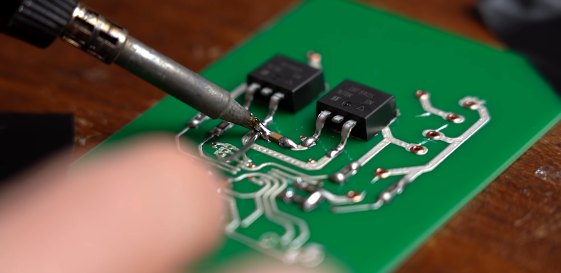
The system relies on interchangeable heads and conductive inks. Mechanically, it doesn’t differ much from a 3D printer. The ink, however, appears to be a little temperamental. On the first test board, one side did not cure properly since [Scott] forgot a step. While it looked fine, it had problems soldering. Because the traces are not copper, the machine comes with its own recommended solder, too.
The most interesting part, though, was when [Scott] tried to port an existing board into the system. He had to make several changes for things like copper fills and via hole sizes. Close spacing required some hand rework, so he probably should have spaced the traces wider in the design.
The printer isn’t cheap and the consumables are rather expensive, too. It is hard to justify the cost just to get fast prototypes that aren’t very representative of a final board. Keep in mind the conductive ink isn’t as conductive as copper and you don’t get niceties like solder mask or silk screening. If you had an active hacker space, a school, or a busy lab it might be worth it to get one-off boards. However, for prototyping production boards, it is unlikely that you’ll want to constrain your final design to the restrictions necessary for the printer. Besides, if you don’t mind waiting for boards — keeping in mind that you can pay to get boards made and shipped quickly if you don’t mind paying more — the breakeven point on the printer is very high.
On the other hand, 3D printers used to be expensive and now they are everywhere. The quality of 3D printing isn’t as good as some other production methods, but it still has a place. So if this technology improves a little and gets a lot cheaper, it could find its way to your workshop one day.
Back in 2015, we predicted that making your own PCBs was getting harder to justify. At the time, many people were unhappy with that prediction, but further decreases in the cost of having boards made for you continue to chip away at the value proposition of making your own boards. Sure, sometimes you just want to do something despite the economics — we’ve all done that. But it does make the economics of PCB printers even harder to work out.


I’ve seen one up close. Is a solid machine, but the price of the consumables is what kills you. From what I remember, the machines where 4k -5k € (an Ok price I guess) but the conductive ink alone, at least from my supplier, where 150 € for 2 cartridges.
For 150 euros, I can do a lot of PCBs in china, with a lot more quality and 4 layers…
What I think is a cool feature is the dispensing, pick and place and soldering capabilities.
So, for creating PCB from scratch is not a good machine. For PCBA is a very interesting option.
I appreciate that the guy took the time to also talk about the challenges he faced too. I was interested enough to look into the specs. Some more details about it in the article about his vid … https://www.elektormagazine.com/news/pcb-printing-voltera-v-one-greatscott. I am still thinking about it. … 4 hours for home-made pcb first time is not bad.
We have one of those in our R&D lab. 4 people tried to do anything useful with it. At the end all of them ordered the boards from a manufacturer. Now we only use it as a drill and heated plate for rework jobs.
Exactly the same deal here. I spent a whole day trying to get it to print a board that I could have build on veroboard in half an hour. It won’t even dispense solder paste properly – it chronically under-extrudes and there’s no software setting to increase dispense amounts. I just laser cut stencils from acetate transparency film, sand it flat and hand paste.
Ah yes, the software. It’s cloud based…
When I used it about a year ago, there was an explicit step in the calibration where you adjusted the extrusion rate to get it to dispense thick enough lines. Also, the software is browser based, not cloud based, which a meaningful distinction, IMO.
Our lab has 3 of these printers and they’re booked everyday. While expensive, they’re amazing a board repair and reflow. If that’s something you would rather do by hand knock yourself out, but once the machine is running, it requires minimal user input so I can work on other stuff.
Highly recommended. Also the consumables are expensive but last a long time (50+) PCB’s.
Pick and place would be a nice addition as a future add-on if anyone from Voltera sees this.
The price (whilst probably justified as it’s a new design) is astronomical – as are the consumables. Reminds me too much of the way current printer manufacturers are exploiting their customers with refill prices.
The base price is the equivalent of having 100’s of professionally made – even for experimentation purposes – pcbs manufactured. Besides, anyone ‘experimenting’ does so on a breadboard these days – why they’d want to make it into a pcb version during breadboarding is anyone’s guess. Layout and tracks can be ‘tested’ in the pcb software you’re eventually going to rely on anyway.
This looks to be the 3D TV of pcb manufacture…….
“you can order super inexpensive boards and have them in very little time”
where ? it costs less than 4€ to make a custom 10×15 board at home. Besides i’m not interessed in ordering 10x the same board when prototyping.
Ok, but 2 layers are allready hard to do at home, especially if you need vias under ICs. Multilayer is not possible, at least not economical.
I still have the gear for etching and do it a few times here and there, but it is just not enough for most of my prototypes. I order mostly at JLC PCB and dont care about the extra boards, just throw them away if you dont want to keep them.
I’ve been doing a ton of PCB-soul searching lately. This looks really expensive and not like a good concept.
So far my heart is going to laser-ablation of paint, and then chemical treatement with HCL, 2 layer is tricky, but via rivets are a thing, and I plan to focus on SMD as much as possible, replacing vias with 0 ohm jumpers.
This seems like the cheapest and simplest solution that fits the work I will be doing.
Have you checked LPKF stuff? They have special paste for making vias – way quicker to use than rivets and can be used under ICs. Their pcb milling machines and laser etchers are great but rather expensive.
I guess I stick with the old photo sensitive process. This seems super super slow, super low detail, not reliable, look ugly, and super expensive. Basically useless. Its even bad for drilling, its super slow, and I don’t think its rigid enough for milling.
It takes less than 45 minutes (not including drilling) to do an up to A4 size PCB with a pre-applied photosensitive film. If you want an even cheaper method, use the laser printer ink transfer method.
Just the heat curing with this machine takes 1 hour per side, which is in itself more than the complete “manual” process of the photosensitive process.
LOL at the home made vs ordered thumbnail. It look more like novelty cake decorations for some reasons. The soldering looks really really bad.
For some reason he insists on manual soldering with a crappy iron instead of the actually recommended process.
No, he just cant solder.
The tip of the iron does look too large, but that might be because of the close up nature of the subject.
My 1.5mm tip looks like a roll-bar under the magnifier :)
The size might be deceptive but it’s definitely the wrong tip for that sort of work.
When I first saw it I thought it would cost maybe $500 or a little higher.
Genuinely shocked at the actual price. The quality of the prints also looks crap.
Toner transfer etc is much cheaper and probably a lot easier.
The ‘special’ blue toner sheets you can buy are also quite cheap if you don’t want to use actual normal toner.
You can get a cheap laminator for about $20 or less.
Only people who like to waste money will get one of these (so they will probably do a good trade with University research departments).
I use normal toner and a beater clothes iron, both printer (with 64% toner left!) and iron from a thrift shop. My secret sauce for excellent results is a little purple glue stick on the paper before printing. After it’s ironed on, water dissolves the glue and the paper comes off clean.
Nice idea. Is the glue the usual PVA stuff?
It seems to me that the “magic” is in the consumables. At the price of them I’m not sure I’d bother with this process at all until if/when their prices comes down. But if I did decide to give it a try I don’t see what’s so magic about their ~$5,000 printer.
I’m sure anyone who has scratch built a 3d printer and is so inclined could come up with a reasonable substitute on a hobby budget. What do we have here, an XY platform. Maybe a Z axis but really just pen up/down. A fine pointed paste extruder on a swapable mount. A small drill motor which can also be swapped in. It’s only for plunging holes straight down so even a cheap harbor freight rotary tool would probably do. Was that a UV light built right into the bed? Ok, cool I guess but a separate UV light box would probably be easier and useful for other projects. I think he mentioned optionally doing solder reflow on the printer. So it has a heated bed. Not exactly hard! Although… I might skip that part and build an actual enclosed reflow oven instead.
Exactly what in this $5,000 beast couldn’t a kid buy from the typical online shops with paper route money?
Software?
I bet FlatCam could do it.
In a pinch, with no time to learn FlatCam or desire to build a whole new machine a 3d printer enthusiast could export a PCB layout to SVG and use one of those online utilities to make a one layer height high STL from it. That could be sliced on one’s favorite slicer and printed on a printer with a paste extruder. Although, a typical printer might not have quite the sturdiness required for the really fine surface mount traces. It should be acceptable for through-hole and larger surface mount pads though.
Wow thats awful. $5000… At ~$5 a pop for a PCB thats a lot better printed from your average PCB shop if you’re ordering 2-4, you’re going to have to get a lot of use out of it to make it back. Thats ignoring that the real fab’d PCB wont look like junk.
“In addition to aligning holes, you’ll need to install tiny rivets for vias and slightly less tiny rivets for through-hole components.”
I wouldn’t say you NEED to.
Don’t get me wrong. I’m not arguing against using modern, double sided construction. I’m just saying, if you are thinking about making your own PCBs but fiddling with rivets or getting the two sides perfectly aligned deters you it doesn’t need to be that way. People got by with single sided boards for decades! You can still build a lot of good projects that way.
Something I think is kind of strange, there doesn’t seem to be much middle ground. Most people are getting their PCBs from board houses now I think. But when you do see a homemade PCB it’s usually either single sided or the builder has perfected aligning the two sides, installed vias and everything. If alignment is hard, why don’t we see designs where both sides are used but connections between are kept to a minimum and accomplished with jumpers, perhaps going through larger holes with no traces up against them so that alignment isn’t so critical?
I agree with you wholeheartedly, I have a philosophy of single side, no holes, to limit additional processing, 1206 0ohm jumpers are a thing, each one saves 1 via, most simple boards will require less than 10 to be done on a single side.
Most people who design PCBs only use them to connect breakouts, connectors and power supplies, which integrate all complexity anyway, high component count, high density designs is something I seldom see.
That goes back to a point I made, though. If you need one board, then lay it out so you can do it with a sharpie, toner transfer, or rub on resist and be happy. If you are making high volumes of prototypes then it stands to reason you are probably wanting to have the board mass produced later. I would hate to tell my clients “This board is twice as large as it should be. I was going to use vias, but I don’t like how my prototyper handles it so I didn’t use any.”
I mean, for that matter, what we used to do for “two sided” was solder a wire through the hole on both sides. You can even do that with some (but not all) through hole components. That was for prototypes only.
So again, it seems like you have two markets: one offs, where it is cost prohibitive and pro prototyping where it doesn’t have enough fidelity to be that useful.
Maybe if you were a rich school where you need lots of one offs and it is OK to constrain the design to meet the tool? That might be a good use case, but most schools can’t afford that kind of consumable budget, I would think.
I always thought if you were a school then the photo-etch was a pretty good way to go anyway – students can own the process all the way through, and its always empowering to see that you can make do with things you can find around the average house, as opposed to using specialist-but-not-really-specialist tools.
Was really stoked when I discovered the laser printer and transfer method.
“Maybe if you were a rich school where you need lots of one offs and it is OK to constrain the design to meet the tool?”
Then why in the world wouldn’t you just get a mill, assuming you don’t want to go the chemical route? There’s literally no design I could imagine this thing being able to produce that a mill wouldn’t vastly exceed, and the ‘consumable’ drill bits are dirt cheap compared to paste.
You don’t necessarily need to worry about alignment for two-sided boards, though – if you only have SMD parts, then just leave the entire backside as a ground plane, and pop rivets in. Poof, all done.
This is a good point, different tools for different jobs, all these PCB manufacturing methods cohabit because people do different things with them.
The one mentioned in the article seems to address almost none that I could imagine though…
For the record my school has an LPKF machine, which granted, is about 10 times as expensive as this one, but produces beautiful boards, very fast, and is capable of doing small series production (probably in the 10 to 20 range) double sided boards with vias, without much user intervention (supposedly it can do chemical via process, but I always used rivets)
Oh, I was definitely only speaking to people making one-offs. I also don’t imagine paying clients who intend to mass produce would be happy about a one-sided limitation!
“Happy” though is not exactly how I would describe my experiences with sharpies, toner transfer and chemicals. Maybe I’ve had bad luck scoring weak Ferric Chloride? Or maybe the stack of old PCB blanks I bought at a hamfest are too oxidized or the copper is too thick. I don’t know. It’s always taken far longer than every book, set of instructions of YouTube video says it should and by the time I get the etched areas down to fiberglass my traces are starting to narrow and pit. I’ve never been happy with the result.
A few years back I decided I was going to develop my capability to produce good PCBs. I got an old HP LaserJet from work, modified a laminator for toner transfer and switched to muriatic acid with an aquarium air pump for etching. That gave me the best results I ever had but still not great. Then the developer went out in the printer. We bought a Brother Laser for day to day printing and it turns out Brother toner is useless for PCB transfers. I still have the HP in case I decide to buy a new developer and have a second try at it. It takes up a lot of space though and I am very tempted to get rid of it.
Meanwhile I’ve taken up 3d printing, built my printer from scratch and from this have been inspired to start collecting parts to build a CNC. I want to skip the chemicals and try milling. If that works well for me then this big printer is gone!
So, for the one-offs being cost prohibitive. Yes, but as I wrote in another post it seems like the magic is in the goo. I’m guessing we can build our own machines to apply it. But, yah the goo is a bit too expensive too, but not so totally out of question as like buying the machine.
Remember those people that claimed to just wipe the unwanted copper away with vinegar and salt? Yah, all I managed to do was turn a board green and that required full on soaking for days!
Was that the pilot of 5-Minute Crafts?
Well, if you watch the video until the end, he´s just sending that crap back to the seller. I guess it will be possible to buy as scrap for little moneyin few years.
Avoid this company!
I was an original Kickstarter funder and waited patiently for an extra year or so until they ironed out the production problems. They originally promised overlapping vias insulated by 3D printed insulator, but didn’t get that to work, so they came up with the double-sided board + drill+ rivets solution. OK, fine, but then they wanted to charge me extra for the drill and rivets. I initially declined, but later decided the drill might come in handy. I have contacted the company several times trying to buy the drill, but they have blown me off. They don’t even offer it as a separate purchase anymore.
I’ve used the thing only once, and and although the circuit board worked initially, one of the vias cracked later.
Honestly, looking at the final product, it does look like a dodgy kickstarter idea…
Oops, I should have said traces instead of vias above.
It’s a neat idea, but I don’t really see the market for this thing.
As has been noted already, getting boards produced is reasonably inexpensive and reasonably quick. Probably not quick enough if you’re a company that wants to iterate daily, but quick enough for hobbyists. If you can’t wait two weeks or so, I’d recommend picking up a second project or another hobby to pass the time. ;)
So, this leaves this printer for these instances where you really need a PCB quickly. It’s quite nice that everything seems well-integrated, but apart from that, I’m not exactly blown away. The biggest problem in my opinion is the lacking ability to produce thin traces. There are a ton of ways to get boards with thick traces, but thin traces are a pain and require optimized processes when doing them at home. PCB milling is a mess, and it’s very hard to produce thin traces with it. Totally possible with etching yourself, but you need to spend the time to figure out your process so you can get 6 to 8 mil traces to work reliably. With etching at home, you can just use more space on the PCB (since large single PCBs are cheap, but panel space isn’t) to layout the traces in a way that doesn’t require too many vias. 0 Ohm jumpers can be incredibly convenient for crossing traces. Of course, the photo transfer and etching are a bit of a pain, and in these times, schools will probably never let anyone get to the chemicals required, but at least for hobbyists, it allows you to design PCBs for reasonably common parts.
However, this printer doesn’t seem to be able to print a PCB for a 0.5mm pitch TQFP or QFN, which I personally would consider absolutely required for any form of serious prototyping, except maybe if you’re doing high-current designs. Pretty much every new chip will be available in a 0.5mm QFN package, so in my opinion, that’s what an at-home prototyping process should be able to accomodate.
This printer doesn’t seem to do it, so I don’t quite see the point. Add to that that curing the ink takes quite a long time, the printer doesn’t seem to have any safeguards against drilling without a sacrificial plate or curing with the sacrificial plate still in place, there’s no automatic drill debris removal, no camera-assisted alignment, everything needs constant intervention and babysitting, etc. Then there seems to be a reason for all the extremely low-melting-point solder used in the video, which is very expensive and doesn’t have good mechanical properties. I guess that you could print a transparency film, expose a photoresist PCB and etch it in less time than it takes the printer to produce it, and with better quality to boot.
I saw the video a few days ago and thought that was way too much trouble, time, and money.
Lately I’ve made several break-out boards (0.5″sq to 1″sq) for soic chips using toner transfer. I used Inkscape (I was lazy vs Kicad), a Brother laser printer, the glossy white peel&stick cupboard paper, and my Weller iron with 1/16″ tip. I can go from print to solder-tinned board in <1 hr.
My process:
a. print the reverse-image on standard paper then peel and stick a swatch of the glossy cupboard paper overtop the image and re-print it.
b. cut-out the image to the size of the board, using masking tape to secure paper around a bare Cu board.
c. place board under cloth rag and hit it with about 1min of heat with a clothes iron.
d. run cold water over the board, gently pulling back the paper.
e. use Cu wire wool to remove the toner while under running water.
f. clean with ipa and tin the board.
g. apply components.
Last week I purchased a hot-air station and went nuts pulling SMD chips from my collection of discarded boards.
I managed to create a break-out board for a 24pin 0.65mm pin-pitch DAC chip with 12mil traces.
After tinning using hot-air, I brushed flux then placed the chip overtop the crowning traces and used the hot-air to let it sink in.
lets just say that i won’t be pouring my feric chloride down the sink any time soon.
A subject near and dear to my heart. I would love for a printing PCB process to work but this is not it. Not even close.
My vision is one that could print resistors and be able to cross traces over other traces (with an insulating layer). Double sided would not really be necessary. Print on bare copper for a real ground plane (conductor/resistor trace on top of insulation trace). Pick-n-place would be integrated in. Place a component with glue. Print the traces to it. Maybe in time it would get to BGAs. All the technology is there though needs a lot of refinement.
And for what it’s worth, I’ve done lots of PCB via toner transfer and won’t ever be going back to that. For $20 and a week, I can get 5 copies of a professionally made 2 sided board of my own design. And don’t have a mini-Superfund site in my house. Milling is slightly less obnoxious (and noxious) but I only do that for a quick proof of concept.
Getting really tired of the product placement for mediocre, overpriced PCB robots on HAD.
Having boards fabricated and making them at home are not the same thing. If I need more than a few or would sell the product, am prototyping for a larger run or want a pretty board then a fab is best. If I am making a one off, single sided with 20mils thickness and clearance rules, then milling on FR1 with an asymmetrical 10°cutter produces a functional board in two hours rather than two weeks. Flipping the board in its cutout outline is alignment enough for silkscreen via laser diode on the same machine then liquid tin for solderability and corrosion resistance.
I just wish we had an online manufacturer here in AU. All the Chinese ones are great and cheap but $5 worth of PCBs costs $16 to ship and you still wait up to 2 weeks for it to turn up. I’d give an Aussie manufacturer $30 Inc shipping to get it to me in 1 week… Assuming Australia Post feels like cooperating that week
I’ve used this machine at my university and the only things that is good about this thing is the drilling part. In my school projects i’ve only had trouble with this thing. It makes a lot of noise, it is hard to calibrate, the dispensing tips breaks easily or gets clogged, The reflow does a poor job and most times the board doesn’t work after reflow soldering. On top of this all accessories are very expensive. Just the dill part costs about 700$ and not to mention tips and solder which also causes trouble. It’s like they built in micro(macro) transactions into this thing.
Get a PCB-mill instead. The actually work nicely and there are a few nice ones on the market.