Physical access to electronics generally means all bets are off when it comes to information security. But in special cases this is just unacceptable and a better solution must be found. Consider the encryption keys used by point of sale machines. To protect them, the devices incorporate anti-tamper mechanisms that will wipe the keys from memory if the device is opened. One such technique is to use a mesh of traces on a circuit board that are monitored for any changes in resistance or capacitance. [Sebastian Götte] has been researching in this area and wrote a KiCad plugin to automatically generate tamper-detection mesh.
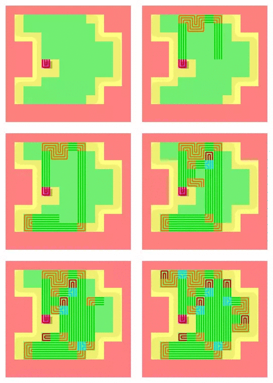
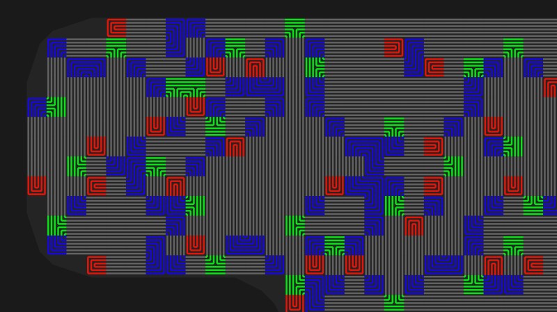
 The idea is pretty simple, place traces very close to one another and it makes it impossible to drill into the case of a device without upsetting the apple cart. There are other uses as well, such as embedding them in adhesives that destroy the traces when pried apart. For [Sebastian’s] experiments he’s sticking with PCBs because of the ease of manufacture. His plugin lays down a footprint that has four pads to begin and end two loops in the mesh. The plugin looks for an outline to fence in the area, then uses a space filling curve to generate the path. This proof of concept works, but it sounds like there are some quirks that can crash KiCad. Consider taking a look at the code if you have the expertise to help make it more stable.
We’ve seen these anti-tamper meshes in practice in the VeriFone payment terminal that [Tom Nardi] tore down a couple of years ago. The approach that [Sabastian] took with the plugin actually produces a more complex mesh than was in use there as it only really used vertical lines for the traces.


I once integrated a bunch of traces below a chemical sensor to heat and measure board temperature. Working well enough. That was hand-drawn Hilbert curve with some mistakes and kelvin connections on the end. Lots of copying.
Hilbert?
Hilbert is not the best option.
You want nearby wires to be from different parts of the length of the wire, so a short circuit is easier to detect.
If it would result in only a small resistance change it’s hard to detect.
You also need to allow for resistance change due to temperature and other causes of drift.
(author of the tool here) A hilbert curve is only an option when you want to cover a square. For arbitrarily-shaped PCBs you have to get a bit creative. Also hilbert curves are 100% predictable, and for some added security-by-obscurity you might want a more random layout.
Checkout this mesh on an actual security chip (via @johndmcmaster):
https://twitter.com/johndmcmaster/status/1334935880134348801
That’s impressive, and also almost seems pointless? I assume the rest of the chip is hiding under the mesh, and this is supposed to stop someone from either messing with the chip while it’s active or from modding it after the fact. I guess what I’m getting at is at this scale, ie chip level small, who would actually attempt to mod the physical circuits when an external hack makes 1000x more sense? And it certainly won’t stop a duplication, that mesh is an acid bath away from revealing it’s secrets.
Secrets are mostly stored in RAM. Dissolving the secrurity wire will make the contents disappear. The chips (how they are built) aren’t that secret the contents are. This mesh will hinder to probe the chip or the read out its memory contents.
(author of the tool here) You are right, you’d use a mesh like this to prevent someone with physical access to your device from reading out secret data such as cryptographic keys.
A common way these meshes are used is that you monitor the mesh for shorts or breaks using some 74-series logic, and when something is detected you short your microcontroller’s or sram chip’s vcc pin to ground. Some microcontrollers also have an “tamper” input pin for this exact application.
Depending on what you are designing, an external attack might not be possible. A smart card, when programmed correctly, will never share its private key, and the only way to get it would be to de-cap the chip and physically probe about in it.
On a similar subject, I wonder if these traces could be layered in a way to produce a nice big capacitor to power a RAM-clearing circuit. A micro-controller that does nothing but iterates through some addresses and writes junk data wouldn’t need that much energy and would severely hinder any form of cold boot attack.
RAM in these systems is usually SRAM and the way it is cleared when tampering is detected is usually by shorting the SRAM array’s VCC and GND lines. In contrast to DRAM, SRAM can be cleared very effectively that way. SRAM does exhibit a small data remanence effect that you have to take care of, but that’s easily done by just periodically flipping and copying data around.
I made similar anti-tamper meshes for a few chips when I worked at Atmel!
In a couple of my meshes, I designed some higher level patterns that should be observable at certain levels of magnification.
“…that are monitored for any chances in resistance or capacitance.” There is a typo there ;)
Got it, thanks.
Can’t wait for Tron Light Cycle game. :P
Visually pleasing, but this is the easy bit. I’d be more interested in the techniques and pitfalls of monitoring these traces.
It’s just a resistor.
You’ll need power (battery, mains power supply) to actively measure it.
But you’ll need power to save keys in RAM also. Putting keys in flash makes this method useless.
There is no need to over complicate this.
A simple circuit is to use a series resistor and use it’s ADC to measure it’s voltage.
To save power, use 2 I/O pins, one to switch the resistor between high & low.
This way you can also detect if a “hard” voltage has been set on the ADC pin.
With a single pin you can also build an RC circuit and measure (dis) charge times.
It’s “just” an antenna – likely a large one.
And as soon as you start pushing current through it it becomes a loop antenna, sensitive to magnetic fields and therefore difficult to shield.
Robert’s question is not at all trivial.
(author of the tool here) The easiest thing to do is to just connect the four traces to four microcontroller IOs and monitor for shorts and breaks. You can go fancier than this, e.g. measuring resistance or even impedance over frequency, but just that basic defense can already be a royal pita if the mesh is any good.
Another use of this is to design heating pads, for example for 3D printers.
If the script is good, it’s quicker then laying out a simple pattern manually, and it looks better.
For increased security you could interweave two or more meshes, and monitor them independently.
(author of the tool here) Using this for designing heaters is a great idea! This script can handle arbitrary board shapes as well as interior cutouts, so especially for irregular shapes or if you want to have holes in the heater this tool might be convenient indeed.
I wanted to just point to heating plates too, now I’m late.
Then: doesn’t this addon already make 2 interwoven meshes? (Read the part about four connection pads)
(author of the tool here) The tool can handle any number of traces. A trace always loops around the mesh, then back to its starting point. That’s why you always get twice as many connection pads as you get traces. If you wanted to make a heater, you could just use a single trace, giving you two connection pads: one for each end of the “wire”. It’s just by default set to two traces/four pads because you can then monitor the mesh for short circuits between the two traces for tamper monitoring applications.
I was thinking that when it comes to protecting the keys to the kingdom, this is pretty weaksauce…far more innovative and sophisticated approaches have been bypassed before.
but thanks to Mike Szczys for linking to the article on the VeriFone teardown! that one explains the goal is to prevent the convenient insertion of skimmers into the device. i imagine it’s pretty effective at that! there’s a world of difference between a persistent threat that just needs to succeed once versus a criminal industry that relies on doing dozens of them every day without getting detected.
(author of the tool here)
Depending on the printing technology you use, meshes like this can be highly effective. For example, I’m not aware of anyone having publicly broken the mesh inside Ingen*co’s current generation of POS payment terminals:https://en.wikipedia.org/wiki/Ingenico#/media/File:Ingenico_iPP350_payment_terminal.jpg
These devices use a FPC mesh that looks like it’s printed in a similar process as the flexible contact membranes used in keyboards, and device and mesh are completely potted in a rubber-like epoxy that tears the mesh traces’ conductive ink right of the carrier foil when mechanically disturbed. Of couse producing a mesh like that is fairly expensive, which is why I focus on simple PCBs right now.
I have an upcoming project where in a couple of months I will share some techniques to significantly beef up the security of homemade security meshes with household ingredients :)
Hopefully it survives lockdown, but if Sylvia Post a pub in SE London actually still has the anti-tamper wall traces from when it was the vault of a post office!
Great fun to try and find the weak spots over a pint :)
(author of the tool here)
The KiCAD bugginess mentioned in the article is a bug in KiCAD’s python interface that affects rendering only. The tool will do its job properly, and the results will render correctly after pcbnew has been restarted. KiCAD’s developers are currently trying to fix the bug since it affects basically every python plugin on 5.99: https://gitlab.com/kicad/code/kicad/-/issues/7065
Hackaday:
Old harware is decaying! We must unite to reverse engineer it and extends its service life!
Also Hackaday:
Check out this cool new plugin to make extra hard any reverse engineering on your projects!
As well…
Monday: Old plastic on vintage hardware decaying, try to save it with retrobrite etc…
Tuesday: Print everything in PLA to save the environment, it rots quicker.
Wednesday: How to back up your data for 1000 years
Thursday: How to permanently destroy a hard disk.
Friday: Run your uC on nanowatts
Saturday: Build a CPU from TTL
:-D
Hmm. Extension to open source program for creating hardware DRM. Is this moving in the right direction? I like seeing KiCAD get new abilities but I’m not sure how I feel about this.
Hardware that can’t be hacked for new purposes when it’s obsoleted from it’s original job isn’t really a good thing. And I wonder about these ideas of monitoring the capacitance of traces for changes. That sounds pretty sensitive. Is it just going to result in equipment that kills itself just because lightning struck somewhere in the neighborhood, the microwave in the breakroom was a little leaky, or someone walked across the carpeted room on a dry day?
Perhaps we could cut out some of the middlemen and production energy use and just pour some truckloads of rare-earth metals directly into a landfill and call it a day instead?
Oh. I guess I do know how I feel about this.
This looks pretty fancy, can we do something along these lines and get nice panelizing in KiCAD?
I’ve only played with the things I’ve seen out their briefly so far and haven’t found a path I like just yet.
POS Terminals / Credit Card Swipes are heavy with security.
International Verifact supplies terminals to banks, card companies, etc. Even customer PIN entry devices use encryption between the PIN entry device and it’s associated terminal. One day they will make the cards secure!