[Markomo] didn’t find much useful information about the Raspberry Pi PIco’s analog to digital converter, so he decided to do some tests to characterize it. Lucky for us, he documented the findings and shared them. The results are in a series of blog posts that cover power supply noise, input-referred noise, signal to noise ratio, and distortions.
There are some surprising results. For example, the Pico’s low noise regulator mode appears to produce more noise than having it set for normal operation. There also appears to be a large spike in nonlinearity around certain measurements.
The finding about the nonlinearity is especially surprising. The converter uses successive approximation to convert an analog voltage into a digital quantity. That’s the method where you generate a voltage using a DAC and compare it to the unknown voltage. In a normal circuit, the DAC would use resistors, but resistors are notoriously low quality on an integrated circuit. What is very high quality is the ratio of capacitor values. In other words, two capacitors might not always have the same value because of variations in silicon dioxide layer thicknesses. But the plate sizes will be right on every time and all the capacitors on the same chip will have the same silicon dioxide thickness. So we might not know that C1 is 100 nF or 220 nF, but if we know that C2 has twice the area of C1, we know the ratio of C2 and C1 very precisely. [Markomo] simulated the circuit and tried varying values until the simulation matched the measured data. The conclusion is that the capacitors on the circuit do not have the right values and are off by just a small bit.
It appears there are a few more posts planned in the series that will cover the input bandwidth, aperture jitter, and the power supply rejection ratio. You’ll want to stay tuned for those.
We’ve been talking about the Pico a lot lately so it is good to see some detailed analysis. We’ve seen other devices on the Pico dissected, too, and we are sure there will be more to come.


Beware the Ides of March!
Any IDEs released on 1st of April are probably a bit suspect too.
I celebrated by stabbing a romaine salad, it lacked croutons and bacon unfortunately.
Even without the condiments, I’m guessing you ate two
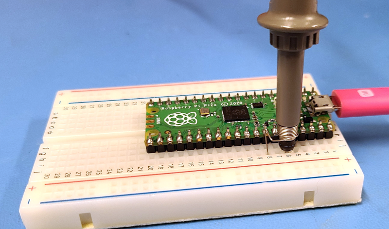
Please don’t tell me he used a plug in bread board to make analog noise measurements?
But breadboards are one of the cheapest ways to make noise.
Breadboards are not that bad for low frequency stuff if you take some precautions.
[Markomo] used a PXIe-5164, a device which sells at 19k€.
I guess and hope that if such a budget is avaiable that there is also enough know how to use it properly.
Al least he uses a proper ground probe. i.e. Not using the wire + aligator clip like the average nomies on youtube.
the problem with the breadboard is the row to row (i.e. neighboring pins) capacitive coupling. For a breadboard, that’s very large capacitance right there – the row contact has large surface area: long and deep.
“For example, the Pico’s low noise regulator mode appears to produce more noise than having it set for normal operation”.
It’s low power mode, not low noise mode. Not surprising that it is noisier.
If it comes to switching regulators and noise there is one source of information which should be contacted first: Jim Williams and his application notes.
E.g. AN101 https://www.analog.com/media/en/technical-documentation/application-notes/an101f.pdf
And, by the way, if you want a DC-DC converter topology which is inherently noisy go for the buck-boost.
> Large numbers of capacitors and aspirin have been expended in attempts to eliminate these undesired signals and their resultant effects.
Pure engineering fun.
Man, having read a lot of application notes recently, especially ones that seem to try to use as much jargon as possible, this one’s levity is extremely refreshing. I read these notes to learn, not to try to parse obtuse language.
>which should be contacted first: Jim Williams and his application notes.
Need a séance for the former. RIP James M. Williams (April 14, 1948 – June 12, 2011)
Precisely the opposite, as I understand it. Low power mode is surprisingly also low-noise mode.
When modeling buck convertors, it’s assumed that noise is reduced linearly as frequency increases. So low-power (low frequency) mode SHOULD have higher noise. But in this case it doesn’t. In this case, low-power mode has lower noise.
A switched mode power supply will induce noise in ( inductive ) breadboard. Semiconductor manufacturers invest millions on Automatic Test Equipment and tens of thousands on their test-fixtures to properly characterise each design.
In measuring input-referred noise, [Markomo] says “Shorting the ADC to ground is a straightforward way to create a low noise input for converters.”.
Isn’t it bad to measure noise at GND (or VCC) level as the measured value won’t go below 0 (or above 4095)?
Really nice work. I like that you not only identified the issue but also the probable cause. I’m a little surprised that a modern part could have such a gross error- amazing. I used to work on pulse height analyzers that measure an incoming stream of pulses to generate histograms of pulse height versus probablility. They’re used in Nuclear spectrometers, the pulse height is proportional to energy. DNL was the key spec, it defined the width of each bin and any errors got convolved into your pulse height spectra and made a mess. There are some ADC architectures that have virtually no DNL (Wilkinson- kind of a fast single slope converter). We were trying to make use of modern, low power SAR converters. The brute force way is get a much higher resolution converter and throw away a bunch of LSB’s. It was common to use a 14 bit ADC for 10 bit PHA. There are also some elegant solutions called “sliders” where you have a precise low resolution DAC fed with random data (maybe 4 bits) and you add its output to your signal in the analog domain before conversion and then subtract it in the digital domain after conversion. It smears the DNL over the sliding range and was pretty easy to do. In the AC domain, there are similar DNL reduction techniques that add noise and then over sample, etc. ADI has some app notes on this. The slider is very elegant since you don’t have to increase your sample rate. In the nuclear instrumentation application- you’re dealing with discrete, asynchronous events and can’t really over sample, etc. Nice work.
Hi John, Good to see you writing about “Gatti” sliding scale offsets for getting good DNL in an ADC. I believe my identification of the problem in the Pico slightly preceded Markomo’s comprehensive analysis. As I had a background of spectroscopic ADCs for X-ray astronomy satellites, it was the first experiment I did with the Pico on it’s backing cardboard as given away with Hackspace Magazine. I presented my findings in a thread on 23rd Jan 2021 on the RaspberryPi forum: https://www.raspberrypi.org/forums/viewtopic.php?f=144&t=299904
Has RPI Foundation made any comment about updating the firmware to correct the problem?
is there anyone could explain to a rank amateur the magnitude of this ADC error?
my use case for these ADCs is for measuring slow moving DC sensor voltages, and real accuracy is not a serious problem, however i would like to know more about how these errors might affect me.
given a DC input voltage between say 0.3 volts, and 3 volts;
1 – what percentage error should i expect, over all?
2 – am i right to think these errors will be at specific voltages, where the wrong caps are?
is any of this documented yet, or will it be?
or am i just not seeing it?
What am I missing here?
Yes the adc has bit gain errors.
So why can’t you multiply top 2 bits by one gain, the next bit by another, and the bottom bits by a third gain?
Multiplication is quick on this chip.
Wouldn’t that fix the adc – assuming all chips are about the same?
With tight assembly code your Python wouldn’t even slow down.