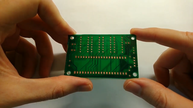
If the last year and its supply chain problems have taught us anything, it’s the value of having a Plan B, even for something as commoditized as PCB manufacturing has become. If you’re not able to get a PCB made commercially, you might have to make one yourself, and being able to DIY a dual-layer board with plated-through vias might just be a survival skill worth learning.
Granted, [Hydrogen Time]’s open-source method, which he calls “Process 01”, is something that he has been working on for years now. And it’s quite the feat of chemistry, which may require you to climb a steep learning curve, depending on how neglected the skills from high school or college chemistry are. But for as complex as Process 01 is, it’s actually pretty straightforward, and the first video below covers it in extreme detail. It starts with a drilled double-sided copper-clad board, which after cleaning is given a bath in palladium chloride. A follow-up dunk in stannous chloride leaves a thin film of palladium metal over all surfaces, even the via walls. This then acts as a catalyst for electroless copper plating in a solution of copper sulfate, followed by an actual electroplating step to thicken the copper plating.
After more washing, photoresist is applied to define the traces as well as to protect the now-plated vias, the board is etched, and a solder mask layer is applied. The boards might not be mistaken for commercial PCBs, but they’re pretty darn good, and as [Hydrogen Time] states, Process 01 is only a beginning. We expect this will be improved and streamlined as time goes by.
Fair warning, though — some steps require a fume hood to be performed safely. Luckily, we’ve got that covered. Sort of.


Impressive. It does make me wonder how it might be possible to modify other photoresist application methods to accommodate this process. I really like the laser printer based photoresist method since it’s so precise.
How much palladium chloride is needed? It’s rather pricey.
Enough to coat the entire board (and container) in a few atoms of palladium.
It’s actually not that much. 20 milligrams are enough to make 50 milliliters of solution that can be reused multiple times and lasts in storage around one year. You do have to buy it upfront, in my case I bought 1 gram of it, but then you won’t need more for a very long time.
Tutorial: palladium
Me and my Wallet: Nope I’m out
Is it less expensive compared to JLCPCB offerings at $2 +$15 shipping? I don’t have a drill (for the tiny vias), hood (for the fumes), chemicals, space, … . Heck it is already bad enough that I have to spend so much time with the CAD layout process.
if you factor in the time you have to spend doing this (you could’ve been something else instead…), no. Not by a long shot.
The closet chemist in me salutes this. The EE in me says, never.
It’s not the expense of the at home method. It is the need to store all of those toxic chemicals, use them, dispose of the waste and clean up the mess. Instead, I just push a button and a week later take delivery of a far better PCB than 99.9% of the hobbyists could make. Even the time saving doesn’t buy you much if you have to order parts to be delivered anyway. I get a Chinese PCB delivery fast than a Mouser or Digikey order.
You can solve al of the deficiencies of the at-home method (PTH, solder mask, silk screen, even gold plating) but at what cost and time?
Home brew PCBs made sense when professionally made ones were expensive and took weeks lead time. The world changed (and for the better in this case).
Too much for me. I’ll stick to single sided surface mount for prototyping. CAD to PCB in 30 minutes.
How about short lengths of wire soldered from both sides?
workable, but a bit of a Pain unless you do some basic think-it-through, ie clip the via-wire short AFTER soldering instead of trying to solder 1.6mm of #30 wire into a via
There are rivets making this easier than short lengths of wire. At such sizes, one can press rivets by hand-force, without a machine. Then soldering them for good contact.
https://pcbprototyping.com/bungard-elektronik/products/consumables/rivets/
“There are rivets”
You beat me to it. However, I have not found a US source of hobbyist quantities for a decent selection of sizes as listed at your link. Digikey only has 1.5 mm OD with none in stock and 7000 at the “factory.” Their minimum order of 500 isn’t unacceptable, but increments of 100 would be better.
Anyone know of a better US source?
1Tone desktop press, cut copper wire, 2 set of custom machined cups (can get away with ballnose endmill for diy) and you are set for life for under $100.
Now this sounds nice for milled PCBs.
That won’t work if the via is also the pad for a component that does not leave space for soldering from the component-side. Moreover, it does not work if the via is under an SMD IC, such as a TQFP or QFN.
Next experiments I’ll do will be to see haw small can I go with drill holes, I have some 0.3mm carbide drill bits to try with my CNC mill.
Basically my goal is to have the same design freedom a professionally made PCB gives you. Soldering wires and rivets can’t do that.
Some wire wrapping would be great for this
Eyelets or hollow rivets. Should be less than a nickel a piece. Used to use them decades ago for this when double sided boards were pricey and took weeks. If you don’t need the hole a wire is fine. But if you need to connect both sides of the board and a header, relay, or something blocking the top is there then an eyelet will allow you to have your hole.
By the time you’ve obtained all the lab equipment, chemicals. weighed their specific gravity, mixed them, cnc drilled the board, masked it, electroplated it, developed it, etched it, cleaned it, inspected it, and soldered all of the five through-hole components, you could have wire-wrapped a dozen of those boards and spared all the economic and environmental impacts.
And what makes this “open source”? Where’s the source? Why has “open source” in the tech world become the equivalent of “here’s how” in youtube land?.. ie clickbait.
Applied chemistry appears to me like it did not enjoy the same sharing of knowledge that software (or even preparative chemistry) did. There are many proprietary formulations and trade secrets that make replicating certain processes at home very hard, essentially requiring one to do the science from scratch.
If you are not interested in replicating this process, a step-by-step guide of the process and the formulas of every reagent may not seem much to you, but if something like this was available back when I started in 2017, it would have saved me years of experimentation to get there.
A 31 step process with a chemical lab VS 30AWG wire soldered on both sides of the board or rivets that can be punched into to it to act a vias. Time is money when you get down to it. If I had to spin a couple of boards myself I would do Mr Carlson’s method or use a PCB house.
How Mr Carlson makes a double sided PCB.
https://www.youtube.com/watch?v=au2ba5gWLWk
It’s all about what the finished product looks like and how efficient the circuit is. Circuits are affected by everything from component tolerances to the vias. Everything in electronics has capacitance and routing of conductors affects capacitance, resistance, and radiant energy. If the circuit is sensitive enough, all of these factors determine if it works or doesn’t. So many times I hear about someone attempting to build a circuit and it fails, they trouble shoot, sometimes with no apparent reason being found for failure. When a circuit reaches a level of complexity to require multiple layers of the board and compactness, it’ obvious such processes are the only option. Here, I commend Hydrogen Times’ knowledge and efforts and wish I had the same. I hate seeing a messy circuit board with wires going hap hazard everywhere. Reminds me of electronics 50 years ago and more. As for YouTube land, some people just gotta pat themselves on the back, some people deserve it.
You can use carbon-based paint (used for ESD protection) instead of palladium: https://blog.honzamrazek.cz/2017/10/diy-through-hole-plating-of-pcbs/
Nope, not really. Palladium chloride is industry standard, and 1g cost of it is enough to cover in copper all your boards, house and neghbours. Carbon produce very bad, fuzzy and uneven surface. Silver nitride is middle ground, but still not nearly as good as palladium.
Palladium chloride’s toxicity?
this sounds so much like the argument for leaded solder and leaded aviation fuel; it’s standard so it is what it is until you realize leaded solder and leaded avgas lets lead go everywhere and leaded avgas specifically is sorta bad for you (yes I know leaded solder is very much safe for the solderer since it doesn’t get hot enough to vaporize)
I am aware of your work, and I would like to ask whether you had success in electroplating small holes (say 0.5mm or less) with the carbon-based paint. Does it flow nicely or the surface tension of the carbon paint clogs the drill hole?
Later, I was able to do 0.3 mm vias. The pain does not flow nicely, but if you suck it with a vaccuum cleaner from the other side, it forms nice thin and even coating. However, it is a long time ago since I did this; I abandoned the procedure and I order my PCBs online. Making your PCBs is just not worth it. And when I am in rush and I need PCB “righ now” it is usually quite simple and I usually designe it to be single-sided or I solder a wire through the via.
What would be the cons of assembling 2 double sided PCBs using hand soldered vias ?
Would it work if we just masked and etched both sides like usual (or in a low budget, using clothes iron and ferric chloride) and then applied a LOT more solder to each pad? I imagine it would flow to the pad in the other side
Thanks for the article, and for the author for sharing it, but the process uses many dangerous chemical products and equipment that are way beyond what I have today at home to deal with.
I’m curious is the next step a 4 layer PCB with blind/hidden vias (or even a 3 layer PCB without blind/hidden vias). Like I do think the pursuit of the knowledge required to do what is currently being done commercially is a noble goal in and of itself. But at the back of my mind also is what is the next step, like I do not envision the final target is going to be a 72 layer F-ALCS PCB’s or even 90 layer PCB.
For all the people suggesting rivets, or wire soldered on both sides of the board, it is just not equivalent to a modern through-hole plated via. Let’s say we want a 0.3mm drill hole with a 0.2mm annular ring, 0.25mm spacing between adjacent vias.
This process of via plating can achieve that. You can’t achieve it with some rivet that is a couple of mm wide and protrudes 0.5mm above the plane of the board.
It’s about having a fabrication process that is equivalent (or close enough) to modern, “real” design rules – and not having to redo the layout to suit the limitations of a very old, very low-tech fabrication process.
You shouldn’t have to change the artwork / design to suit the limitations of your prototyping process – that kind of defeats the purpose of building a prototype of that given layout.
Would simpler processes (direct copper plating perhaps?) work if the holes are vias only, thus don’t need to stay open?
Tons of comments about rivets and this and that. What’s the problem with getting your boards done professionally FOR $2!! Shipping is usually around $15 to US. Delivery in about 1 seek. In this way, my “prototype is near production ready also.” I mean, making your own copper-clad board would be “cool” also, but … Why? …. Why?… TWO DOLLAH !!
Sometimes you need a board that is larger than a business card.
That’s something I am finding, with a project that involves a lot of connectors so there really isn’t any way to make it smaller than the sum area of the connector bodies. Once you get past those little demo-project board sizes the price seems to rise very quickly. And I for one don’t really like spending large amounts of money on something that is essentially a prototype and might not even work on the first run if I failed to catch any mistakes.
Also, I often think that maybe if this community wasn’t so hooked on using board houses people would be a little more liberal with their use of PCB real estate. In particular I would like to see mounting holes make a comeback. Too many little devices are sold as raw boards and then if you want to make a case for it you have to design in clips. What a pain, all for the lack of a little corner space and a hole.
But then, this process looks like too much chemical work for me and for most of my projects I can live w/o plated holes just fine.
I can get my boards up to 100mm x 100mm (what kind of credit card is this size, I wonder?), “2”-sided, for “2” DOLLAH. No chemicals needed. If I need something bigger, I just find a good subdivision point and make “2” boards and connect them together. There is something magical about “2.”
Some of the boards I’m doing are 500mm x 300mm. Most PCB houses don’t support boards that size.
BTW, instead of using mounting holes, I would use chemicals (epoxy, super glue, or …?) and just glue the board and case 2-gether. It should not be 2 hard 2 do.