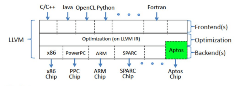
Everything is better when you can program it, right? We have software-defined radios, software-defined networks, and software-defined storage. Now a company called Ascenium wants to create a software-defined CPU. They’ve raised millions of dollars to bring the product to market.
The materials are a bit hazy, but it sounds as though the idea is to have CPU resources available and let the compiler manage and schedule those resources without using a full instruction set. A system called Aptos lets the compiler orchestrate those resources.
If you are astute, you’ll see this has some similarity to RISC and even more to VLIW computer architectures. For more detail, there’s an interview with the company’s CEO over on TheNextPlatform which has some insight into how the CPU will work.
In addition to RISC and VLIW, transport-triggered architecture shares in this philosophy, too, although there have only been a few commercial versions. So the idea of pushing work to the compiler isn’t new. Time will tell if Ascenium’s approach is really different and beneficial or, at least, if they can make more of a mark against the three or four big CPU makers.
Of course, if you really want to reconfigure your CPU, you could do it with an FPGA. Transport-triggered architectures have an advantage there because all you have is a single instruction along with addressable units. You can even microcode those for more complex instructions or emulations.


Sounds midway between Transmeta and an FPGA. Super interesting!
Wouldn’t that be an emulator? Could dynamically reconfigure sections of it.
This sounds interesting. Almost heading to a virtual cpu. Could this be the end Moore’s law. ?
>Could this be the end Moore’s law. ?
No. It already ended.
But McQuitty’s Law is still alive and well: No matter how fast the computers, it’s still too slow.
I’ve not heard that one. Nice
+100
Law #2 the day your O/S works the best is the day support ends and a new buggy version is rolled out.
If their technology has any promise at all then the company will be bought by AMD or Intel.
…or Apple.
Just what we need. The most perfect solution to cross-platform support being locked behind a platform that is opposed to cross-platform in every capacity.
Imagine this thing being 100% restricted to running MacOS and programs signed by Apple and written by devs who’ve paid their annual license fee.
Aren’t Intel chips translating x86 instructions I to the native instructions with the microcode blobs? In a way cpus are already programmable.
True, but the end user can’t reprogram them.
Itanium rises from the grave! https://en.wikipedia.org/wiki/Itanium
It’s not quite dead. Intel said they will cease production on July 29th, 2021
Some ex-Transmeta folks designed the Denver2/Carmel CPU that turns a VLIW instruction set into ARMv8. https://en.wikipedia.org/wiki/Project_Denver
Unless there’s an order of magnitude performance improvement, power savings or something otherwise phenomenal, it’ll be difficult to upset the momentum behind established architectures and manufacturers.
They are claiming higher performance and lower power.
If you read their 2005 paper they were talking about 64 multiply–accumulate operation per clock cycle. And if you look at page 15 that pdf paper, in simulation, it is an order of magnitude faster than a dedicated DSP chip at performing DSP operations while being clocked slower and using the same power.
It does sound interesting, but so too did the Mill architecture ( https://millcomputing.com/topic/on-the-lack-of-progress-reports-from-the-mill-project/#post-3702 ) And at least there was actual good public information about the Mill architecture, there is very little public information about the Ascenium Aptos.
Looking back at how something stood 16 years ago is not all that relevant from a performance and power efficiency standpoint today.
Since one do have to make a lot of design considerations surrounding the actual manufacturing node one will use for making the chip. This means that performance and power efficiency isn’t strictly inherent in the architecture itself.
Also, I should point out how the number of hardware execution units for a given instruction in hardware isn’t really dependent on the ISA, but rather its implementation in hardware, especially if one starts tossing in out of order execution. And also has pros and cons associated with having more or fewer copies of an instruction.
Then there is the question of how many instances of an instruction is actually needed, eventually the bottleneck isn’t the instruction throughput, but rather the decoder, or out of order queuing system, or just the ports that sends off the instruction to the specific execution unit. (To a degree, this is related to the whole RISC/CISC debate.)
It was around 2005 when processor clock speed hit their maximum (There have been no 10GHz or 100GHz CPU’s). This is because power consumption is proportional to the clock speed squared. You want to switch faster you got to pump in exponentially more energy, and then you need to remove the heat generated before the silicon turns into lava.
We currently have no economic cooling solution available to remove the watts per square centimetre of heat from a silicon based chips to increase clock much faster than we have now, so instead the clock speed was limited, and in reality reduced. The power required to switch faster can be reduced by making feature set on the chips smaller (lower capacitance, well total gate charge), but then you have more thermal energy being generated in a smaller area (higher watts per square centimetre), so it is one step
They currently pulse higher (turbo) until thermal overload is reached and then that core is seriously under clocked until cool enough. This allows for faster startup times, also to gain higher benchmark results, and a bigger marketing number on the side of the box.
Performance in recent years has been increased by using more parallel cores, and power has been reduced by clocking them slower on silicon with a physically smaller feature set.
In a superscalar CPU the dispatcher reads instructions from memory and decides which ones can be run in parallel. In the above processor it lowers the complexity of the dispatcher and decides at compile time what instructions can be run in parallel. That will inherently take more time and use more power at compile time, but if the compiled binary program is run on millions of CPU’s around the world, that is where I see the biggest power saving. Which would do a better job, the compiler with access to all the information or a very complex dispatcher with limited knowledge.
I can see some merit in the the above chip, but I wish that there was more public information.
The problem of doing scheduling at compile time is though that it largely requires knowledge of the specific core that the software will have to run on.
Ie, targeting a wide range of processor cores would require individual compilations of the software, making software compatibility a bit of a pain to deal with.
But a complier should already as is do most of the scheduling, the out of order system should only really handle the last few tens of instruction calls in a thread.
The advantage of having the last bit of scheduling done in the core itself at runtime is that it brings forth the ability to both run with SMT, and to more gracefully run through an L1-L2 cache miss without instantly stalling as a result. (SMT’s ability to interleve two or more threads is giving us even more time to avoid stalling a core, and context switching is having a fair bit of associated overhead so SMT is a far more valuable feature since it allows one thread to stall for a bit without wasting core resources.)
Doing all of the scheduling at compile time has its pros and cons.
And in the current market, there is frankly more deficits to what I can see. Considering how memory bandwidth bottlenecks have been a staple among CPUs since the 90’s, more cache only partly solves this issue, where some applications practically don’t see any improvements from more cache. And the larger instruction calls associated with doing the scheduling at compile time is going to increase the memory bandwidth requirement for a given workload.
In regards to power consumption, it only partly scales at the square of the clock speed. Since the transistor stages themselves generally transitions at the same rate, regardless if the processor is running at peak operating clock speed or completely idles. But the short term average power consumption will however be greater if one switches more often, resulting in larger currents and thereby larger conductive losses. And there has been improvements here, what used to be a 60+ watt chip now gets beaten by the SoC in a midrange phone that barely breaks 5W.
Power consumption and heat isn’t strictly the main reasons clock speeds haven’t improved. But rather that there is other ways to improve overall performance in a system in ways that doesn’t have the same deficits as increasing clock speeds. Multi cored CPUs is the real thing that stole the spotlight as far as power efficiency goes.
Memory latency is also one of these pesky things that gets progressively worse with increasing core clock speeds since we run more cycles in the same amount of time. This latency can be partly circumnavigated by prefetching, sometimes speculatively.
Having more cores running at a more moderate clock speed results in fewer clock cycles for us to prefetch over, reducing the amount of speculation needed, and thereby getting better guesses and less wasting of bandwidth. And if we stall, then it isn’t the whole processor. Together with SMT, the core itself might still have a similar throughput. And here core level scheduling has the advantage of being able to pick up the slack with the other thread.
Then there is also SIMD instructions increasing the workload fairly substantially, even if the core runs at the same clock, it can handle a good amount more data in a given clock cycle than what used to be the case.
There are however situations where going with compile time scheduling has some improvements, this is mainly in applications where we look at pure serial performance. Though, in most cases, just giving the thread its own core and telling our kernel to not switch it out even if it stalls, tends to offer up fairly large improvements as is. And rarely would a realistic workload need much more than this. And if such is the case, then a more application specific accelerator might be more suitable regardless.
For general purpose CPUs, it is however rather advantageous to let the CPU core do some of the scheduling itself.
Gotta read more in depth, but from the article alone it seems they want to apply the RISC motto (use a simple instruction set, let the compiler optimize the best instruction order) to superscalar architectures (let the compiler choose the optimum number and type of execution units and how they are scheduled).
Typical downsides would be:
– Worse code density, because the instructions have to encode common operations in more detail. This leads to needing larger memory and caches.
– Lack of binary compatibility. If they add a new module (e.g. new parallel ALU) to a CPU model, all existing programs have to be recompiled.
I have designed a few TTA CPUs (and have a patent on some features of one of them). They are nice because each execution unit has an address on the bus so as long as you don’t remove/change what’s there it is easy to add to it or even extend execution units in compatible ways (e.g., add a new register that wasn’t there before).
Been in two company that done that previously, both being failures (in the product term).
Why do they think they can succeed this time?
Because someone is dangling a few million dollars in investor dollars in front of them, perhaps??
Both companies burned more than that…
Because general purpose CPUs are meh. Not interesting. Nothing new to do in this market. And application specific compute accelerators only starting to be commercially viable (not counting the GPUs, of course). Look at all the inference and crypto accelerators out there.
Such architectures are very beneficial for compute accelerators, and pretty much useless for the general purpose.
Well there’s always adding specialized chip-lets to the fabric. Getting the best of both.
Isn’t this just the same sort of thing as Taos’ virtual processor? It was pretty impressive at the time (saw it on an ARM/x86 pairing), and I think when they abandoned it, they moved to using their technology for JVMs.
Here’s a link to a Byte article about it from 1991: https://sites.google.com/site/dicknewsite/home/computing/byte-articles/the-taos-operating-system-1991
It wasn’t abandoned; it was used all the way to the end until the company collapsed, at least in the second generation form. (I worked there right up until the end.) That article describes the earlier form, VP1. That actually started life as a complex set of macros for an existing assembler — it was incredibly simple! VP2 was much more sophisticated, with an unlimited number of virtual registers, expression tree representation for, er, expressions, and, eventually, strong typing.
We did have a chip design house get really excited about it and got into talks about producing a CPU which ran VP2 natively. However we kept having to tell them that there was really no benefit over an existing CPU architecture.
Apologies, my poor writing/editing – I meant that Taos operating system was abandoned (at least, I understood it was when they went towards JVMs). I may even still have the dev kit on a couple of 3.5″ discs somewhere…
Technically — yawn. As others said: microcode, WLIW, Transmeta. All of this has been coming and going as the ratio of CPU-to-storage bandwith changed over time.
What is changing more is: desperate investor capital in search of shiny ideas. So what counts nowadays is idea marketing, not the idea itself.
The sad part (I don’t mind those with the money playing casino) is that this mindset also pollutes free software and maker communities. Every newer project resembles more and more a marketing campaign these days.
Strange times, where each discovered vulnerability has a logo and a web site.
So now a program can take down an entire OS?
Also a security nightmare, with infinite bug possibilities.
What about wear out with time?
Not worth the effort, stick with GPU with many ALUs.
The lesson from the Itanium debacle was that the compiler can not schedule execution units precisely. It’s better to leave it up to runtime and do it in the CPU, as at this point also the input data is available (in contrast to only code at compile time).
It is generally advantageous to let the CPU handle the more nuanced instruction scheduling.
Since when the CPU core does it itself then it opens up the door to a lot more nuanced instruction layouts. For an example how many of each type of instruction one should have, without having to worry about software not being supported just because one lacked that “n-th” adder that it expected to be there.
Sending additional data in regards to execution unit scheduling would result in larger instruction calls without much benefit outside of a few niche situations where the hardware scheduler isn’t up to snuff, or where the scheduler results in too many clock cycles per series instruction for one’s liking.
Since most CPUs do not execute fully serially dependent instructions even close to core clock. Even with speculative out of order execution. Non serially dependent instruction however can be executed in parallel. And here another concept comes in to bring up that “instructions per cycle” rating of the core, and that is Simultaneous Multi Threading (SMT).
And scheduling execution units between two or more simultaneously running threads that at times have nothing in common is not fun to do when one complies, since one has no clue what the other thread(s) are up to. Even if they are part of the same program, it can still be hard to know what branches they have ventured down without asking, and asking takes time and resources. (One can split the core in two, but then one has half the performance all the time so what is the point?)
Then there is the whole part about compiling the code in the first place. If one just leaves execution unit scheduling to hardware at runtime, then the complier can just “not care” about that part of the process and simply set its effort on making the machine code itself as good as it can. But if it also needs to consider execution unit scheduling for improved performance, then compile times would likely increase, and at the very least, one wants to be on par with the hardware scheduler if not even beat it.
So in the end.
Scheduling execution units sounds somewhat nice at first glance, since one can optimize the code a lot more and reduce the length of the execution pipeline in the core.
But the increased size of the instruction calls, dependence on the layout of the core, and the issues surrounding SMT is major downsides. Not to mention the obvious, if one runs on a more powerful CPU with even more execution units, then one can’t use those benefits unless one recompiles the whole program again…
I can though honestly see a few subtle advantages in regards to exceptionally serial programs that needs the peak serial execution rate to be as fast as possible. Then there is advantages to removing the whole scheduling/out-of-order part of the core as to reduce the number of clock cycles per instruction. But this is really niche considering how most computers can just schedule more CPU time to a thread instead. (A CPU runs thousands of threads, and only has a few cores to run them on, it is a game of whack a mole in regards to tossing out stalling threads and replacing them with new threads with their data in order, until they too inevitably stalls after a few hundred or million cycles. A thread needing good serial performance could just be given a core of its own to run on constantly, even if it stalls. This though eats cores for breakfast… So far from practical for most systems.)
Sounds a lot like the Linn Products Rekursive CPU from the 1980’s
Rekursiv was a computer processor designed by David M. Harland in the mid-1980s at a division of hi-fi manufacturer Linn Products. It was one of the few computer architectures intended to implement object-oriented concepts directly in hardware, a form of high-level language computer architecture. The Rekursiv operated directly on objects rather than bits, nibbles, bytes and words. Virtual memory was used as a persistent object store and unusually, the processor instruction set supported recursion (hence the name).
By the time the project had delivered its first implementation, new processors like the Sun SPARC and Intel 486 had surpassed its performance, and development was abandoned in 1988.
https://en.wikipedia.org/wiki/Rekursiv
There’s other companies doing that already, being to market, and offering things already, Codasip for example.
The main reason people are once again looking at shifting decoding to the compiler is side channel security hacks. We have processors capable of so much, but we keep on having to cripple them because of side channels hacks. Context switches that require cash flushes, branch prediction disabled etc etc. All the significant security failures of recent has one common component: real-time hardware allocation. It’s sad, but its the reality. The final cost will significantly include a reduction of code compatibility within a family of processors, or an increace in code size to accommodate various hardware options. The benefit will be a more predictable, less hackable system.
This really isn’t like Transmeta or any of the code-translating CPUs before. It seems more like Adapteva’s Epiphany CPU, which has thousands of simple cores, translated down to the ALU level, but then the weird thing is that they’re running from a single instruction queue.
There’s a presentation from 2019 here: http://chipex.co.il/_Uploads/dbsAttachedFiles/PeteFoley.pdf
That does a much better job of explaining things in my mind. It’s interesting because I kinda feel like a similar architecture might be a better fit inside an FPGA for stuff like high-frequency low-latency stock trading to replace the existing DSPs in there (likely with far more multipliers), since the existing DSPs in an FPGA are really fairly limited in how you can extract parallelism with them.
That’s just an updated version of what ARM has been doing, X200 from XMOS as an example
The Gray-1 is another variant on the idea of defining a CPU in software. https://hackaday.com/2017/02/02/the-gray-1-a-computer-composed-entirely-of-rom-and-ram/ If once the CPU starts it loads everything into RAM then you can also have a self modifying CPU, that perhaps optimises itself over time to match the work asked of it, e.g. by also collecting statistics at runtime as to what it is doing.
They will simply fail except in cases where performance is not an issue. Remember that Thorvalds left Transmeta in 2003. It’s a beautiful idea, but stupid.
What about bit slice?
How similar is this to the B1700 architecture?
It is totally different than the B1700. On the B1700 the compiler for each supported programming language compiled to a predefined instruction set specific to the needs of that language & compiler, and the B1700 microcode was switched dynamically to emulate the instruction set used by the program currently running. There was no attempt to globally analyze program flow and create an instruction set/data path optimized for the specific program rather than the general needs of the programming language. The only program-specific optimization that I recall was that, because there was not a fixed word size or instruction length on the B1700, address fields in the generated instructions contained only the number of bits required to address the number of variables declared in the program. Also, the B1700 was a uniprocessor, whereas the Ascenium hardware is an array of 256 relatively simple, 32-bit processing elements.