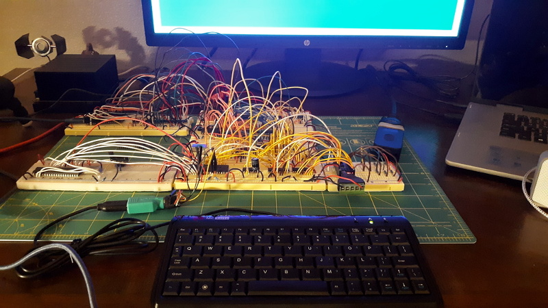
If you’ve ever worked on a system that loads its software from a ROM or EPROM, you know how much of a hassle it can be to make frequent changes to the code. Pulling the chip, flashing it, and sticking it back into the socket each time you change a line isn’t anyone’s idea of a good time. Which is why [Nick Bild] has come up with the PicoROM, a way to emulate a ROM chip using the Raspberry Pi Pico.
With the Pi Pico standing in for the original ROM, updating firmware takes a fraction of the time and doesn’t require you to actually disconnect any of the hardware. [Nick] had done something similar with FPGAs in the past, but the far cheaper and easier to work with Pi Pico makes this version particularly appealing. The secret to getting it to work is the overclocking potential of the Pico, which he says has been pushed to 400 MHz for this particular application.

The downside is that you can’t access the Pico’s onboard flash when the chip is running that fast. To get around that limitation, all of the code is loaded into the microcontroller’s RAM. With a healthy 264 KB of memory this isn’t really a problem when emulating 32 KB chips, but [Nick] says his method would quickly fall apart for larger ROMs.
Beyond the Pi Pico itself, [Nick] is using a trio of 74LVC245AN 8-bit logic level shifters so the chip can talk to the 5 V logic of his homebrew 6502 computer. With everything wired up on a simple breadboard, PicoROM has no trouble serving up the operating system as it hums along at 2 MHz.
Of course, a modern high-performance microcontroller isn’t strictly necessary. In the past we’ve covered devices that could emulate an EPROM using 1990s era silicon.


Next step : build a slightly adjusted raspico DIP40 compatible and replace the CPU itself … (PiStorm…) :-)
Hm..400Mhz to serve a 2Mhz CPU. 20Years back we could do this with a static Ram and some Register. The world did not become smarter in the last years.
Olaf
I think the point is to simplify the ROM development process. Compile your rom, build your Pico image, deploy over USB to the Pico and reset your retro machine. Certainly a lot better than unplugging/erasing/programming/plugging.
Sure you can do this with battery backed up SRAM, but you’d still need to build the usb programmer side of things.
For four components with a BOM of maybe $6, why bother?
Sorry Olaf but you don’t seems to understand the complexity of this.
Single use purposely made electronic it’s always faster then programmable electronics, they are way more simple, the world has become faster in the last yers because we figure out to do a 400mhz programmable microcontroller order of magnitude smalled then the 2mhz one.
It’s like saying that the brain of a insect react faster compared to a human one, it’s just becase it’s smaller, yet, the human brain built a 400mhz microcontroller chip, the insect it’s still feeding on carcasses.
No, I understand it. The traditional way in doing it is using a static ram and some logic. You load the binary with a serial port to the logic and than the logic switch the static ram to the bus. This was normaly used >20years back when people did not like to burn an EPROM all the time. I remember 1 or 2 two circuits for it the electronic magazine of these days. You can complayin that you need externel logic, but the new PICO needs external logic for buslevel translation, too.
And of course I understand if a microcontroler has not slave-memory interface it needs to be VERY fast to serve as a slave. This is the reason there existed at least two microcontroller with this interface (8042 and a special Z8) But they are two old and clumsy to server a 6502 well. :-)
BTW: I wonder if it is not more convienent to pull the 6202 out of the socket and emulate it directly with the PICO.
Olaf
For the commodore there is KungFu Flash which is an ARM stm32f40something clocked at 168mhz which does a lot more decoding then just a read/write signal.
I agree with Olaf that 400mhz is way too much to emulate an EPROM.
You two know no one it’s forcing you to do it? instead of being happy about a new exciting opensource project you find what’s wrong with it?
if you are so incline in this toxic approach to thing, fork the project and fix it.
Seriusly, wtf.
From the github:
Speaking of processing cycles… I have been using PicoROM with a 2 MHz system clock with perfect stability (the 6502 accesses memory in half a clock cycle, so it’s really handling 4 MHz access times).*** I’m not sure how far it can be pushed*** , but it is handling my current requirement with no problems.
My emphasis.
On another note, I ask because I don’t know, could any of this have been done with PIO and DMA? Would if offer any advantage?
There are a lot of toxic comments on this site, but I certainly don’t think these are them. Pointing out another way to do something that is orders of magnitude simpler is warranted, helpful, and even a running joke on this site (see 555 timer). Olaf’s suggestion was pretty common in the 90’s for tuning EFI sports cars, so there are a fair number of commercial products to do this.
The project is great, and I very much appreciate the ingenuity of this solution, but it is fair to point out that a 400 MHz microcontroller is not the only choice for someone just trying to emulate a 2 MHZ ROM (and is even a bit comical). This is especially true on a vintage platform where learning about the various support chips and logic ICs is part of the fun. But so is learning to program a modern microcontroller, so to each his own.
You could have typed your comment into a commodore 64 but instead you chose something with far too much power for interpreting keystrokes.
If retro.hackaday.com would be up to date and would support commenting i would do it on my Tandy 1000 with Arachne. :3
+1
More than 30 years ago I did similar things to Z80A targets with a 8031 as programming slave. Basically you just have to behave like a bus-master DMA device – tell the CPU to “shut up” and do your own stuff. The 8031 was chosen because of its architecture and the built-in serial port. The target needed only minor modifications like stuffing RAMs in the EPROM sockets and some additional wiring.
It might be not that easy with the primitive 65xx, but dual-porting some fast SRAM is always possible and it comes with a benefit: if used as RAM you can inspect its contents in realtime without disturbing the CPU.
I like this. It does the job.
Is it the most efficent way to do it? No.
Could it be done better? Certainly.
Does it get the job done for [Nick]? Apparently so.
How many of us have quick’n’dirty hacks that start off just as a proof-of-concept and then stay that way because they fulfill our requirements?
My suggestions how it could be improved if one wished to do so:
* PIO together with DMA chaining
State machine reads the address lines and writes them to its Rx FIFO and tries to pull from its Tx FIFO (block).
DMA is set up (beforehand) to read address from Rx FIFO and write to XXX_READ_ADDR_TRIG of a second DMA channel
2nd DMA channel reads abyte from the address just set and writes to SM’s Tx FIFO
SM unblocks, reads the byte copied by the 2nd DMA channel and puts it on the data pins
The memory holding the EEPROM would have to be aligned to a 32K boundary (for a 32K EEPROM) and the top-most bits pre-loaded into the PIO register before shifting in the address lines.
* Link the EEPROM data in directly rather than setting each byte individually in code
The GNU linker will happily convert a binary file into a linkable object file (using the ‘-r’ parameter). This can then be declared as an external array in the C code.
I’ve played a little with PIO and DMA on a Pico so although I haven’t tried this specific thing, I’m reasonably confident that it would work (might also be worth using a pin for /CE rather than constantly just blindly reading the address pins). Assuming it does work, it offloads the entire functionality to the PIO and DMA hardware. The main CPU is then effectively idle.
Even if using PIO is not possible, turning off USB support will probably help somewhat as it’s not used but will presumably be eating some cycles. Alternatively the EEPROM code could be started on the second core.
Can I ask your thoughts on how (if?) you would use PIO with external serial to parallel/shift registers, maybe with a buffer to separate clock domains? Figuring one may need more pins.
I appreciate this uses more stuff than the original project, and therefore kind of defeats the point, but it does seem like an interesting topic.
Thanks.
I’ve not used any of these types of EEPROM chip so I don’t know whether it’s normal to just hold /CE and/or /OE permanently low or toggle them as required for each byte but ideally you’d have (probably) /OE as a trigger. Otherwise you’ll probably find the address bus changing half-way through shifting (which may or may not be fatal depending on timings, latches etc.)
My initial approach to using a shift register would just be to have the SM toggle the clock pin to the parallel->serial shift register for the address bus and just use the ‘IN’ instruction to shift each bit in on the appropriate edge of the clock (possibly with wait cycles if necessary).
Writing the EEPROM byte to the serial->parallel shift register would be the same but with the ‘OUT’ instruction instead.
I don’t think the overall logic would be that much different but it would obviously be slower as you’re only shifting one bit at a time rather than 8 or more. You’d have to make sure you kept to the timings in the EEPROM datasheet as to how soon after a stable address the data must be available.
In case anyone’s interested, I coded this up using PIO and DMA (https://github.com/rhulme/picoROM_pio).
There’s definitely a performance boost. I haven’t compared it directly against the original code but from the timings mentioned, I think it’s hitting around the same performance without any overclocking.
Nice project. I have used commerical units that work like this often over the years, and of course hardly ever now that EPROM/s are essentially never used in new equipment. Using what you have on hand, and are up the curve with is definitely the way to go with any project. Who cares if a multicore ARM on a raspberry pi is massive overkill, it is on hand and affordable. All the units I used to use had serial interfaces, with your choice of ARM board, you could be using the network.
It is all about getting the job done at a reasonable cost with reasonable effort. And having fun.
Amiga CIA chips and kickstart roms like this would be epic.
Unix in rom will be very atractive idea
This is pretty great. I’m looking to emulate some much larger (64mbit, or 16meg) ROMs – any idea if this is feasible with the same technology? I can already see that a lack of GPIOs is a stumbling block but if anyone else has successfully done this in the past…
I wonder if the Pico flash memory can be extended through swapping RAM into ROM via the GPIO pins (or any USB hub) to an external memory device (SD card, or something?).
The code it would take to make an SD card work, might make up for the lack of space it has in ROM.
What do you think?
I gave this a modified go (I tried including /OE behaviour) but I think I’m pushing it too far with my 6502 system. I’m running the 6502 at 6-7MHz and I couldn’t get the Pico to serve up the start address for FFFC/FFFD requests. I think I’m going to be forced into coming up with a PIO solution.