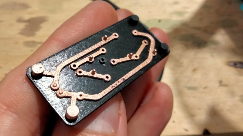
Conductive filament exists, but it takes more than that to 3D print something like a circuit board. The main issue is that traces made from conductive filament are basically resistors; they don’t act like wires. [hobochild]’s interesting way around this problem is to use electroplating to coat 3D-printed traces with metal, therefore creating a kind of 3D-printed circuit board. [hobochild] doesn’t yet have a lot of nitty-gritty detail to share, but his process seems fairly clear. (Update: good news! here’s the project page and GitHub repository with more detail.)
The usual problem with electroplating is that the object to be coated needs to be conductive. [hobochild] addresses this by using two different materials to create his test board. The base layer is printed in regular (non-conductive) plastic, and the board’s extra-thick traces are printed in conductive filament. Electroplating takes care of coating the conductive traces, resulting in a pretty good-looking 3D-printed circuit board whose conductors feature actual metal. [hobochild] used conductive filament from Proto-pasta and the board is a proof-of-concept flashing LED circuit. Soldering might be a challenge given the fact that the underlying material is still plastic, but the dual-material print is an interesting angle that even allows for plated vias and through-holes.
We have seen conductive filament used to successfully print workable electrical connections, but applications are limited due to the nature of the filament. Electroplating, a technology accessible to virtually every hacker’s workbench, continues to be applied to 3D printing in interesting ways and might be a way around these limitations.


For those that are interested in the process, I wrote a bit more about it here: https://projectquine.substack.com/p/the-printn-plate-series and will try continue to document things as I improve things.
Thank you for sharing the project page! I added the link, it’s exactly the kind of implementation detail we love to see!
Maybe link to the original source?
A messy option is to also electroplate the component connections to avoid solder. Looks like a challenging hot mess for real-life circuits, but intriguing. NurdRage used it to make a high-temp bond to a hot-plate temperature sensor at about 5:20 https://www.youtube.com/watch?v=vLEo57DXgiE
Yeah, its definitely possible to plate the components directly into the circuit. I did that for some of the through hole pins and on a basic resistor. I haven’t tried it with the full circuit but I think it should work :)
I recently mistakenly ordered some conductive epoxy capacitors from digikey. They don’t have solderable leads: they’re intended purely for conductive adhesive construction. I didn’t previously know this was a thing, but it’d sure be an easy way to address this. Tough to rework, though, but at least they’re as cheap as typical SMT caps.
If you want to see some state of the art copper 3D printing, check out Markforged’s Copper material for the Metal X. They were able to achieve almost 99% pure copper. Considering the feedstock composition (ie, not using powder!) and the fabrication method, it’s pretty impressive. One of the ways they were able to achieve this is through an additive in their feedstock that dissolves in opteon. Then for sintering, they used machine learning to determine the scale factors based on piece geometry and material. They report they’re able to achieve 84% electrical conductivity.
It is almost like Markforged marketing found this page, but does not realize no one here can afford their $100k printer or proprietary materials. In other news, I can go 200 mph, if I only buy a Ferrari first.
If I have $100k, I could have board house do their fast turn around for me for the rest of my life and still have money left over. I can even get some CM to stuff the boards. :P
The Markforged machines look amazing, I get a bunch of very targeted youtube Ads recommending them to me. Definitely something I would like to test one day, but probably currently out of my price range :P
It’s very nice but $300 for 200cc of the stuff is absurd.
Clever
The problem with electroplating is that you have to connect up *every* traces you want to plate.
If I have understood your comment correctly, a solution could be that if you designed the contact point for the electrode as a test point, all individual traces could be connected to the electrode separately?
Yeah, this is kinda what I have done so far. I add in additional vias/test points into the traces and then have pins that make contact with them. I am currently looking at ways to improve this because the pins bond to the trace which is not idea and makes it more difficult to automate :(
What’s the use case for this? Where would someone use it? It is certainly interesting but no competition for a traditional PCB.
And, btw, all wires have some resistance. Extruded ones just tend to have higher resistance than copper. Though, that makes them printable resistors which could be interesting by itself.
hey Phil, yeah it definitely won’t be competitive to getting a board fabricated. the immediate usecase is simple prototyping of basic boards, but it also allows one to design the electronics into the actual model and is not constrained to 2D, so you could probably do some designs that are impossible with traditional PCBs.
The main reason for exploring this is that we are looking at how we can make a 3D printer that can completely replicate itself, so one of the main hurdles is to be able to print a motor. I’m hoping to be able to 3D print n plate coils that would allow us to make an axial flux motor of some sort. We are not really worried about size or performance at the moment, but looking at what is currently possible.
You can do a lot more with flex or rigid/flex PCB. :P Sometimes they use flex PCB to fit electronics into tight 3D space of a camera.
Printing a motor would be quite a feat. Traces will carry several Amps. Neat if you could print that.
As to fast prototyping, how would you would hook up finer pitch SMDs – 0.5mm pitch or finer. Or, BGAs? Impedence matching? Strip transmission?
Also, what is the finest trace width that is practical now?
Don’t get me wrong, I would love a machine that could pop out a prototype. I just think there are a lot big hurdles.
For this to really be interesting we need hot-ends that can inject powder into it. This way you can make select sections of your 3d print conductive by injecting graphene which would make electroplating much more interesting.
Having 2 extruders and only using conductive filament in the trace extruder would allow you to dip the whole board in the electroplating bath and make the whole board in one go. No need to worry about making them removable or plating tiny pieces individually, and that conductive epoxy mentioned earlier would take care of the solder. If the board is perfect and “cheap” enough, you wouldn’t need to rework it, just print a new one.
Just had a thought: if you stuck a non-conductive layer in the middle and ran through-hole vias, you could even make a double sided board. You could probably do more layers if you were willing to glue some of them together after they were printed and plated. I wonder if this is worth trying.
Yeah it’s definitely possible to make multilayer boards, especially if one has an IDEX 3D printer. You could even do double-sided boards a bit easier by just making a model that prints on one side and then is foldable :)
You don’t need double sided. Just print an insulation layer on a trace and run another one over it.
yeah, having two extruders would be ideal, I need to get around to adapting my 3D printer to an IDEX dual extruder setup. That would allow me to make much more sophisticated circuits, even printing in “resistors” and capacitors by selectively covering parts of the conductive PLA.
Currently my approach with doing it in layers works pretty well and I can dip the whole board in the bath and plate it all at once, provided I plate the plating pins at the right places, but there is still a lot to experiment with and improve.
I am sure most will slap their palm on thier forehead in a Picard manner. But why can’t we 3d print solder?
Thats not such a silly idea, there is actually a company https://www.voltera.io/product/pcb-printer which I think is doing something close to that. I think the problem with just pushing solder into a 3D printer hotend is that it would probably just form droplets rather than a paste. I might be possible to extrude solder paste and then later heat it but I think it would be hard to get the solder to stay where you want it in both cases. But there might be clever ways around that :D
Thank you for reply. I have seen tiny balls of solder when people do BGA could we not feed that into the hotend?
It’s the other end that’s the problem. Solder has a really high surface tension, so like water coming out a fine nozzle the stream breaks up into beads. In this case, the solder would likely bead up and cling to the extruder nozzle rather than cross the gap to the target.
You’d need something the equivalent of soap in water to stop the beading.
I use a process to 3D print my circuits like breadboards, and then “sew” in cheap cat5 wire to form the traces. I mostly use it for making RPI breakout boards.
https://bitbucket.org/mndes/hatrdashery
Nice, that is super cool! definitely will give that a try!
I’ve seen antennas created with genetic algorithms that look impossible to construct. IIIRC, one looked a lot like a piece of low density steel wool. This method could make these accurately and easily. I like it!
100% I think there is some interesting applications if you couple this with optimisation algorithms. The flexibility of FDM coupled with the properties of copper or other metal plating could be useful for all kinds of things!
You can use carbon conductive spray paint to get the base layer of your electroplate conductive rather than the conductive filament. Since the bulk conductivity is low with the filament and you’re depending on the plate it is a bit more cost effective.
I have played around with conductive spray paint too, but its not as easy to get the traces to go where you want them. One of the goals of the project is to eventually make this fully automated so that a 3D printer could print parts/circuits for itself and plate them. I have been wondering if some kind of conductive pen might work slightly better as we don’t need a very thick base layer to plate onto.
The copper plating will then depends on the adhesion of the spray paint onto the surface.
This is an awesome project, but I find it unfortunate that you use Substack to document such a project when Hackaday is a much better and more suitable platform.
I have been thinking about starting to keeping project logs on hackaday as I go along and then having the longer form stuff on substack as I find it better to write there. Thanks for the feedback!
This is quite an interesting way of making PCBs, and might be feasible for the average maker, if the issues of “easier” electroplating and solderability can be fully worked out.
For the latter, there are solder alloys out there with liquidus points at lower-than-usual temperatures, even below 100 °C, many of them with significant indium and/or bismuth content. But these are not common, and I’ve no idea how much any of these would cost, nor whether they’d be suitable for bonding electronics.
I’ll be starring the Github project page, to keep an eye on progress made, and might even experiment with the method myself. Best of luck to hobochild!
Yeah I think with some improvement it would be a great process for the average maker to have in their skill set. What’s interesting is that it allows one to design your electronics directly into models and you are not constrained by 2D pcbs, so you could start seeing some pretty cool projects born out of this. I have been experimenting with low temp solder which reflows at 138C its still a bit hot but it seems to work pretty well and doesn’t affect the underlying PLA model too much.
The PLA doesn’t warp badly at 138 °C‽ I haven’t tested this myself, but I’ve read it can soften in structural/mechanical applications at temperatures as low as 40 °C.
Can you not just 3d print a foil stamp, and then stamp iy onto copper foil, perhaps using heat to fuse to the plastic? Then peel off, use a negative stamp to ‘cut’ the foil between the stamp ridges.
I think you definitely would be able to do that. I know there was a guy doing something similar using a resin 3D printer to etch PCBs, here’s a thread where he walks through it: https://twitter.com/RealTimeKodi/status/1454830940090507266 . Definitely an interesting direction to explore!
The ‘plastic melted by solder’ issue could be turned from a bug to a feature: 3D print a 3D freeform trace network, electroplate it heavily, then melt out the plastic to leave a self-supporting metal network.
100% love this idea. It would be super cool to have free standing trace networks. I have been experimenting with doing a melt out ( you can see one here: https://twitter.com/ProjectQuine/status/1467814199946584066/photo/3 ) but the PLA expands pretty substantially. Maybe if I had a kiln and could get the heat up super fast so the plastic liquidised super fast then it wouldn’t expand as much, but I don’t really have a good understanding of thermodynamics so who knows if its possible :P
Surely for that nozzle one you can print sufficient voids and buckling lines into the PLA that it can expand internally without bursting the shell?