While there has been no shortage of FPGA-based recreations of classic processors, we always enjoy seeing a new approach. Last month [Some Assembly Required] took on the challenge to recreate a classic computer from the ground up and started with a 6502 implementation in Verilog. You can see in the second video below that he’s made good progress and there are apparently more videos to come.
The ROL instruction is the subject of the second video. We liked the approach of looking at what the instruction does and how many cycles it takes on different variants It is always good to make sure you know exactly what you are trying to accomplish before you get started.
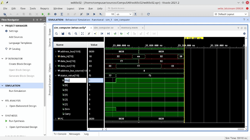
We also like that the tutorial used some of the more interesting features of Vivado like automatic verification. Even if you are experienced with Verilog, there are some good tips here.
In the end, he’s still a good way from his final goal, but it looks like he’ll get there and we’ll be interested in seeing the rest of the video series as it completes.
The 6502 is a popular retrocomputing target. One of the tools this project uses is the Visual 6502 which we’ve covered before. That same simulation has ARM1 and 6800 targets, too.


One of the shift functions was missing from the 6502 originally. There was a workaround, I think I saw it in Dr. Dobbs. A check says the ROR had a bug, so Mos Technology acted like it didn’t exist.
It was gone after a few months, so not only did they fix it, but it took very little time.
It is a great project. I do wish that someone would do an FPGA of the 6509. They are next to impossible to get and would be really handy for the people that have any of the B/CBM II computers around.
I just had a look at the architecture and that would not be a problem. It’s quite a simple CPU with a few quirks like all old CPUs.
The problem I saw is with this document
http://archive.6502.org/datasheets/mos_6509_mpu.pdf
The print quality on page 9 is very poor and that page is really important if you’re writing a HDL equivalent.
I did an FPGA of the whole 65xx family. Just lookout for “MockA65xx”.
Errata 9+3=C (not B)
If you look as the Z80 instruction set you will see the easy ways to do instruction decode. It’s basically 6 sheets of 256 op-codes (16×16) tables on order of the op-code and it makes the decode obvious.
There isn’t much as far a HDL is concerned for the Z80 as the original (and current) spec is a right pain in the ass for timing cycles due to the inbuilt dynamic RAM refresh. I’d like to abandon the refresh as no one uses DRAM anymore and try a single cycle synthesis.
You can try single cycle, but it might add enough complexity to limit your frequency. A reasonably pipelining may get you more throughput at higher frequency.
Pipelining would be better overall if you wanted equal length instruction cycles as it would be less waste to waste one pipeline state for branch instructions.
Z80 has limited onchip registers, so you’ll likely run into memory references on instruction stream. You want to squeeze those into a single cycle? Better off pipeline them so that you get some concurrent decode/operand fetch/execute in parallel and some how get close to 1 instruction per cycle. We know we can get there with x86/x64.
It all boils down to speed vs complexity trade offs. At some point, that’s the path forward.
I’ll Probably start with a standard 20MHz hardware CPU. Z84C0020
There’s some HDL cores in development and some are targeting up to 240MHz. If they can achieve that then I won’t bother writing one.
Most try to be 100% compatible which means including DRAM refresh which will never be used at these speeds.
The problem is that if you abandon compatibility then you have so many decision to make before you start.
I wasn’t too worried about speed/complexity tradeoff. The Z80 is small for a modern FPGA so I would go all out for parallelization and speed.
The thing I loved about the Z80 (and 86 series) was the use of ports, rather than memory mapped IO.
When I heard the M series ARM core was available for FPGA, I wondered if it could be modified to include port IO. After all, there are opcodes deliberately left available to linking multiple CPUs.
Alas, my ideas outweigh my programming skills.
What is the advantage of ports over memory mapped io?
It depends on which side you’re on. I remember the 6502 being introduced, and it was a benefit. While CPUs with i/o ports, it was better.
I/O ports don’t clutter the address space, memory mapped keeps everything the same so every instruction works.
I/O ports were fine for small systems like the Z80 because they simplified the address decoding. A memory 74138/etc could be enabled by /MREQ and an I/O 74138/etc enabled by /IORQ.
However, separate instructions were needed to cope with the separate address space. And in larger systems like ARM, that’s one of many hindrances it brings. Address decoding isn’t a problem in modern systems and address map capacity is usually excessive for the application.
The Z80 had 2 port instructions:
Out (C),n … Out (C),A etc
Inp C, n … Inp (C),A etc
And I think INDR, IND
And these or any instruction that used the C register to index 8 bits of the (port) address, would also use the B register for the other 8 bits or the (port) address bus.
So if you only used these (C) instructions then you had 65536 (2^16) ports, otherwise you only had 256 (2^8) ports.
The other instructions used 0x00 or 0xFF as the other 8 bits depending on if it was a CMOS Z80 or a NMOS Z80.
I can understand that 8-bitter has limited address space, thus doing memory map requires decoding more address bits to not waste the 16-bit space (i.e. more complex decoding logic).
Some of the more contemporary chips/MCU/soc have larger than 16-bit address space and/or onchip peripherals or programmable chip select pin with programmable range/address, so this has become a moot point.
I like memory mapped I/O better because there is no difference between memory space and all the same memory instructions can operate on I/O as if they were in data. Same thing for those annoying Harvard architecture that exposes and force the use of code/data space. The hardware can be implemented that way, BUT also hide it so that it doesn’t need to get in the way of coding.
If I remember correctly there was no invert bits function. You had to perform an XOR with #FF which accomplished the job.
Was that a thing on other CPUs? It wasn’t a bug on the 6592.
Why not the “W65C02 Soft Core (RTL model)” diretly from WDC?
https://www.westerndesigncenter.com/wdc/w65c02s-core.php
Let me count the ways.
First, this is a commercial product, and mine is a hobbyist project.
Second, this is a 65c02, where down the road I may need 6502 behavior. For example, the GEM interface on the C64 used some 6502 unofficial opcodes that were a result of the gaps in the decoding tables.
Both those points could be negated simply by using one of the many open source implementations.
Last, but by no means least, because then I wouldn’t have the joy of implementing it myself.
Because the fun is in the design process, not the end result.
I haven’t seen tasks being used for much more than simulation.. actual synthesis ? no… It seems to defeat the purpose, doesn’t it ? what are your thoughts `?
I’m interested to hear as well.
I find the reaction to this project a fascinating case study on the differences between classical FPGA programmers and myself, a fundamentally software developer doing FPGA programming.
On the official level, Verilog actually has pretty well established guidelines on what is synthesizable and what is simulation only. Tasks are perfectly fine for symthesized code, assuming they don’t do stuff that is, itself, non-synthesizable.
Of course, if you’ll excuse me for using software terms, the synthesizer has to inline everything the task does. So far, Vivado has not had any complaints about having to do so.
The end result is that the tasks do not cause the core to be more efficient[1]. They do little more than just organizing the source code. As a software developer, however, that is quite a lot, in and on itself.
In part 4 of this 3 parts video about the ROL command I’m intending to show how this allows us to implement almost all other variants of the ROL command with about two lines per variant.
You need hardware interfaces rather than software interfaces, but all the concepts work. So, all addressing mode tasks leave the address in which the operand resides in the data latch, and the operation is decoded into a dedicated register.
I haven’t gotten around to optimizations yet, but I have high hopes this will also allow reducing the number of LUTs used without resorting to dumping precompiled tables of microcode into the Verilog source code.
I doubt this will end up being the most efficient FPGA 6502 implementation out there, at least as far as number of logic gates used is concerned, but it might just be the most versatile and most readable one (at least to software developers).
With that said, I really do want to hear Al’s take on this question.
1 – I said tasks do not make the core more efficient. In one way this isn’t 100% accurate. Tasks mean that the same operation is done exactly the same way everywhere it is needed. This increases the chance that the synthesizer will be able to collapse those operations into common logic.
Task internals will not be ‘reused’ in hardware like a function call is reused in software. Ultimately, if you have a signal such as ‘address_bus_source’ that is assigned in various tasks, called in various places, it will end up as a single register, with a bunch of logic for the data and another bunch of logic for the enable signal. The logic will combine all the cases in the design.
For instance if you write:
if( a )
do_x();
else if( b )
do_x( );
and do_x does something like x <= 0, y <= 1, then the synthesizer will translate this as:
if( a | (~a & b) ) x <= 0
if( a | (~a & b) ) y <= 1;
I’m wondering in what way what you said is different than what I said.
I’m getting a bit ahead of myself, here, but what I’m planning the final code to look like:
if( a ) do_x();
else if( b ) do_x();
else begin
x <= 1'bX;
y <= 1'bX;
end
which gets expanded to:
x <= 0;
y <= 1;
You said “the same operation is done exactly the same way everywhere it is needed”, I’m saying that’s not true, because ultimately it’s only needed in a single place, in front of the register that holds the bits.
your final code will probably look more like:
if( a) do_x();
else if( b ) do x();
else if( c ) do_y();
else
x <= 1'bx
where do_y() does something else, so the synthesizer will be forced to implement all the logic.
Look at your 'address_bus_source' for instance. It gets assigned different values in different tasks, and the task is selected based on the opcode and other state bits.
That means that the register for each bit of 'address_bus_source' will need a combinatorial tree that includes a (partial) instruction decoder. Basically, the synthesizer will copy all the conditionals down to the leaves of the assignments, flatten the whole thing, and then try to optimize.
For some reason I can’t reply to your comment.
I was trying to condense a half hour video to a few lines of comment, which is probably why it didn’t turn out coherent enough.
If you look at the 65c02 opcodes chart on page 22 (https://westerndesigncenter.com/wdc/documentation/w65c02s.pdf), you will see a certain pattern. For example, the high nibble of all load instructions is either A or B, and low nibble of all LDA opcodes is either 1, 5, 9 or c.
(except LDA (zp), which is an opcode that didn’t exist for the MOS 6502).
Likewise, you’ll see that all absolute addressing opcodes are in columns c, d or e, and only in even lines.
What this means is that, when decoding, you can check certain bits of the opcode in isolation from the rest of the bits. This greatly reduces the size of LUTs.
For the MOS 6502, as well as for most FPGA implementations, this is done by employing a two stage lookup table. The first one looks only at those bits, and the second one uses the results of the first one to decode the rest. I have several issues with this approach:
1. It is extremely inflexible. Things like introducing the LDA (zp) command, turning unknown opcodes from “undefined’ to “NOP”, and filling columns 7 and F with new commands mean this optimization simply doesn’t work any more.
2. It is unchangeable.
What I’m aiming for is letting the synthesizer figure out these optimizations, where they are applicable, on its own. There are some preliminary indications that I’m not totally delusional on that front, but, of course, I might be wrong.
What this means is that I’ll be able to use module parameters (documented on the github page at https://github.com/CompuSAR/wd65c02, but not yet implemented) to change the behavior of the CPU. This means the same code can produce MOS 6502 compatible or W65c02 compatible implementation, as well as implementations not compatible with either, but that are smaller in size.
I hope I’ve made what I was aiming for clearer.
I don’t write Veralog. Instead I chose VHDL and *this* is the reason … it looks TOO much like sequential code and some of what would otherwise be called “compiler directives” seem at though they may be runtime synth.
Keep in mind that I don’t read Veralog so I’m trying to interpret what you mean.
To me it looks like the question your asking is …
If you have a number of subsets of combinational logic that are dependent (for input) on a common state machine, then, is that state machine duplicated for each subset of combinational logic.
Well, If the state of the state machine can be different for each subset of contamination logic then the current state (prior to any state transition) can be registered separately for each subset however this will NOT happen without a load pulse or clock domain.
So unless you specifically code a load pulse and registers (i think you use the @ for edge trigger) then then when it is “flattened” it will just cause a number of iterations of the state machine.
To use an example more relevant to CPUs.
If you have two general purpose CPU registers (B and C) and the ALU can preform the functions Load, AND, OR and XOR on any one of these along with the an Accumulator register (A) and leave the result in A then of course you will need an RESULT register to transfer to A and a load signal will effect the transfer.
The slow way (and common way) to do this is have the ALU select the function (Load, And, OR, XOR) and the source (B or C) then transfer to the result register on a load pulse.
The faster way to do this is to have 8 registers R1 – R8 where
R1 = B
R2 = C
R3 = A . B
R4 = A . C
R5 = A + B
R6 = A + C
R7 = A (+) B
R8 = A (+) C
and select which R (R1 – R8) goes into the result register or simply to A with a multiplexer.
BUT!!!
this will “flatten” or synth down to the “slow” way UNLESS you have a clock (edge trigger @) that loads into R1 – R8
So it depends on your code. In most cases things flatten down unless you make an effort to make it do otherwise.
The synth will always flatten combinational logic but it can’t change time domains or register loads.
Hi RÖB,
I’m not sure I followed what you said, but I don’t think we’re speaking of the same thing at all.
First, regarding the directives: the only one I can think of that might look like a run-time directive is the readmemh one, and that one’s only executed in the “initial” block. In other words, it’s used to load initial values into registers.
If you try to use it in an always block (i.e. – as part of your logic), what you’ll find is that, when you try to synthesize your design, it will fail.
Which is, really, my answer to all of your reservations. The build tools know what the hardware can’t do, and is pretty vocal about letting you know when you stepped out of bounds. Which, to me, means that you can step as close to the edge as you like, you’ll know when you overstepped the FPGA’s boundaries.
There are a couple of things about Verilog you seem to not know. The first is that, at least Vivado, will warn you sternly if you have a logic loop that does not have any flip-flops in it (aka “asynchronous loop”). You can only make that happen if you ignore those warnings.
The second has to do with the difference between Verilog and System Verilog. In the later, there are constructs that guarantee the logic will be in a clock domain (called “non-blocking assignments” in Verilog), and constructs that guarantee asynchronous logic (“blocking assignments”). If you use them, it is illegal to mix blocking and non-blocking assignments.
In other words, if you use the tools correctly, it is impossible to get it wrong by accident.
As for the “sequential code” comment: I think that’s a good thing.
When you design a circuit, you can do either forward reasoning or backward reasoning on it. Forward reasoning means you say “when this happens, I want that to be the result”. Backward reasoning is “I want that to be the result when this and this and this happens”.
Designing with logic gates uses backward reasoning, so most hardware engineers find it more intuitive. But real life isn’t designing backward.
When you create a 7 segment decoder, you don’t start with “let’s see what numbers cause segment 3 to turn on”. You write down all the numbers, and choose which segments are on for each number. That’s forward reasoning. You then use a technique, employed mindlessly, to convert that to backward reasoning so you can write out the logic gates needed.
This is 2021. Why employ mindless techniques when the computer is perfectly capable of doing that for us?
The things hardware engineers find most appalling in my design is that fact that the same register gets assigned multiple times, which by Verilog logic means the last assignment is that one that will actually happen.
But I’d argue that’s a /good/ thing. It means I write what I mean, and I trust the synthesis tool to figure out how to turn that into logic.
Trust me, there is no danger of anyone mistaking this for software. I say this because the Verilog tutorials I learned from treats the language as a software development language. I have made mistakes. Oh boy, have I made mistakes…
But Vivado was very clear that they were mistakes. You hit “synthesize”, and your mistakes are reflected back to you.
You can treat Verilog as a software programming language. For writing simulations, I do just that. Getting the simulator to load the test-plan from memory file, and then assert that the CPU behaves like the test plan says it should would have been considerably more difficult in hardware.
But when you write for FPGA, the tools are very clear about what you cannot do. I see no fault in having a tool that is more capable than what you can use, so long as you can clear boundaries on where you shouldn’t go.
And Xilinx seem to agree. In fact, they offer to program FPGAs in C++ now.
I understand what you’re saying about making the design simpler, but the problem is that it can expand in large logic blocks because all of the context of the call needs to be propagated down and copied for each of the state bits. In your code, there are many state bits that depend on the full instruction decoder, but it’s not immediately obvious when just looking at one of the tasks.
The risk is that this process happens implicitly, so you’re not really aware of the impact which means the design can get very big.
As a comparison, here’s my own 6502 verilog code: https://github.com/Arlet/verilog-6502 using an intermediate state machine. This means that the logic that determines what happens to, for example, address bus bits does not depend on the instruction decoder, but on the internal state machine, which is smaller. I agree it’s less flexible when you want to add an instruction, because you have to update the core in various places, and maybe extend the state machine. The synthesizer is not smart enough to perform such transformations. When you’re done with your design, I recommend looking at the resource use, and then download my design and compare.
I actually looked at your implementation before I started mine. For some reason, I couldn’t get it to work, though it might just be because I was a total novice at the time (as opposed to a relative novice, which is what I’m now).
I’ll definitely compare them when I’m done. If you like, I’ll drop you a note when I do. It’s probably still a few months in the future.
One thing you’re wrong about, I think, is the state machine claim. I do not, in fact, decode the opcode every cycle. During cycle 0 I decode the opcode into two state registers, one for the operation and one for the addressing mode. I am hoping, though have not verified it yet, that this will serve the same purpose as the two stage lookups that are traditionally done for decoding the 6502 opcodes, without the rigidness that come with it.
I do, completely, see in my future the need to tweak the precise values each enum of those states get, in order to help the synthesizer to unify bits. I still think that’s a more readable, more flexible solution than hand coding the entire state machine.
I don’t like them, because it makes the design look too much like a software project, instead of a hardware description. Assignments to the same flip-flop are scattered throughout the source code, hidden deep inside tasks, which makes it much harder to visualize the synthesis result.
Any project on a super optimized best of and enhanced 8bits CPU design ?
More registers, more RAM, more IPC, would call it Z8509 …
I would make it a fully 16 bit design with 16 or so registers. There will be a small cost for wider datapath, but bigger savings in reduced control & decode.
Why not, if we can ensure a decent level of binary meta-compatibility with 8080/Z80/6502/6809 ;-)