Most of us are familiar with the concept of producing PCBs in a panel, and snapping them apart afterwards. V-grooves that go most of the way through a PCB are one way to go about this, but a line of perforations along which to snap a tab is another. But what’s the best size and spacing of holes to use? Sparkfun’s [Nick Poole] spent some $400 on PCBs to get some solid answers by snapping each of them apart, and judging the results.
The nice thing about creating a perforation line (or “mouse bites”) is that drill hits are a very normal thing in PCB production, which makes creating this kind of breakaway tab a very straightforward and flexible method. However, it can be tricky to get results that are just right. Too sturdy, and breaking apart is a hassle. Too weak, and the board may break or twist before its time. On top of that, edges must also break cleanly. We’ve covered panelizing PCBs in this way before, but this is the first time we’ve seen someone seriously look into how to create optimal breakaway tabs.
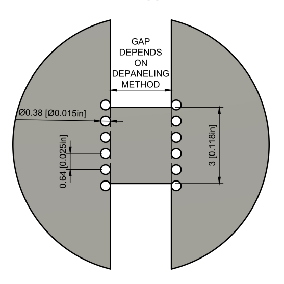
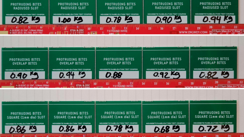
Data on designing mouse bites was sparse and a bit inconsistent, so [Nick] decided to figure it out empirically and share the results. The full details are available in Building a Better Mousebite (PDF download) but the essence of the recommendations are: 0.015″ unplated holes, spaced 0.025″ apart (center-to-center), tabs a maximum of 0.118″ wide (so as to be compatible with depanelizing tools), and holes that extend into the corners of the breakaway tab to avoid sharp edges. Holes should be placed slightly differently depending on whether one wishes to optimize the cosmetic appearance versus the physical smoothness of the board edge, but those numbers are the core of the guidelines.
To fine tune, [Nick] suggests increasing the spacing between holes to add strength, or just adding additional tabs. What about thickness of PCB? [Nick] tested boards both 0.8 mm and 1.6 mm thick, and while different amounts of torque were needed to snap the boards apart, things still worked as expected regardless of PCB thickness.
When it comes down to it, the best numbers will ultimately be the ones that your process or fab house can most efficiently handle, but [Nick]’s numbers should not steer anyone wrong, and it’s fantastic to see this kind of work go into refining such a common PCB feature.


About 20 years ago, I worked for a company that made a high volume telephone dialler product.
After about the first 100,000 were produced, we found that we were getting some unusual failures.
After some analysis we found that these were units that had been located in cold and/or damp locations, such as a basement or an old house with solid walls.
We finally tracked it down to some 0.1uF 0603 decoupling capacitors, that were being damaged when the pcbs were broken out of the panel. Microscopic cracks were forming inside the capacitor, and in damp/humid condtions the capacitors were absorbing moisture and, worst case, becoming more like 1K resistors.
Line powered devices rely on the 50uA that you can draw from the phoneline to keep them powered. The failing caps were causing our power reservior capacitor supply to discharge in a matter of minutes.
The solution: any SMT decoupling caps that were close to the pcb edge were turned so that their long axis was parallel to the pcb edge, so the stresses of depanelising the pcbs did not damage them.
It’s definitely worth remembering that MLCC caps are quite fragile if they’re placed somewhere that can flex them, even a small amount. I remember Dave Jones had a PSU catch fire on his bench due to a cap being placed directly between two screw terminals, with essentially no stress relief for when when those terminals were tightened down.
https://www.youtube.com/watch?v=VwdnGbI5ls8
For these reasons, we use mousebites designed specially to be removable using wire cutting pliers. Causes next to no stress on the PCB and does not protrude out of the PCB.
can you give and example illustration of this arrangement?
“About 20 years ago, I worked for a company that made a high volume telephone dialler product.”
Let’s get him!!!!
Forget the mousebites. Just design small tabs and get some depaneling pliers. The end result also look better.
And as noted in above comment; take care about those ceramic caps near any stress points. It’s a common failure cause…
Great info! Thanks for providing the details on this.
I’m just a home hobbyist. After stumbling around for a while trying to figure out how to depanel boards myself, I ended up buying a Harbor Fright metal shear, and simply cutting the PCBs apart. When I need pretty edges, I smooth them off with a belt sander.
I do this *before* the boards are assembled, to avoid any stress on components.
Have you been spying on me?
The above procedure works really well for be as well. The shear makes a clean cut with an effective kerf of 0 unlike when I used to use my band saw.
I find it quite wasteful to order all those PCB’s just to test mouse bites.
I’m guessing sparkfun uses a lot of panels anyway and these tests could easily have been combined with PCB’s that end up in real products instead of the garbage bin.
I also find their single recommendation doubtful.
Mousebites that combine 20×20 PCB’s in a panel very likely have a different geometry then mousebites that hold just 3 PCB’s in a panel.
Mousebites can also easily be a 2nd or 3rd choice.
There are also quite a lot of PCB depaneling tools:
https://duckduckgo.com/?q=pcb+depaneling+tool&t=h_&iax=images&ia=images
The simplest are hand pliers that can nibble a small piece out of a PCB while tools for doing bigger batches can be pneumatically or electrically driven.
A big concern about the design and use of such tools is to reduce the bending of the PCB. As stated before, bending the PCB during depaneling can easily lead to damage. SMT resistors and capacitors are quite brittle. IPC also has guidelines for footprint to edge distance (for different depaneling techniques) and rotation is also a significant factor.
I also once read on the KiCad forum about some company who bought such a cheap chinese router just for depaneling PCB’s.
If batch size allows, an automatic depaneling tool could even be integrated in a PCB test jig.
The Idea is, you put a panel into a test jig, and you take tested and separated PCB’s out of the test jig.
For a company that is also paying for every hour invested in the experiment, $400 is probably cheaper than adding the testing conditions to all those products which might end up being discarded if damaged in the process.
Having done PCB’s for volume manufacturing in the 10000’s i have found that normally the correct pcb breakaway (rat bite) tabs are born from looking at the whole PCB assembly process from SMD placement, Auto insertion, conveyor movement, solder reflow and ATE test. Ease of breakout is nice and less damaging but the whole PCB manufacturing line should be considered. If people are interested i have a openscad PCB model here https://www.thingiverse.com/thing:3819822 with DXF measurements. This was used for single sided / double sided and 4-Layer PCBS at high volume mostly 1.6mm thick.
Maybe of some help. The model is semi parametric but being openscad you can re-configure and view before any commitments.
Awesome, thanks!
“drill hits”? :)
Problem is that if you go to some place like JLCPCB for instance, the operators will regularly override your mouse bite designs with their own, and not even consistently use the same pattern. I’ve also gotten boards from Eurocircuits that use faster/cheaper tooling for their mouse bites, resulting in visibly wonky positioning.
Remarkably, when I submitted a design to jlcpcb with mouse bites they came back in precisely the location I had specified. Weird.
Maybe that was an irregularity?
The difference can be subtle. I found out because I downloaded the manufacturing version of the gerber files, and compared them with the ones I submitted.
I use a metal brake to cut PCBs. It is fast and leaves clean edges. Grizzly has a good shear/brake for $244, I have the $344 one.
I’ve worked 15 years making boards in PCB fab, and from that 7 years actually panelizing boards for customers as a CAM/CAD operator. The suggested mousebite pattern in the whitepaper is a thing of fantasy, where all isolating routings are not made with a round bit, but with a square bit instead. You can’t use small 0.4mm drills to make the tabs, because you need the diameter of a bigger hole, so you can fit the routing inside and not end up with the devils horns after the customer breaks the board apart.
I’ve found the most effective mousebite patters to be made with 3 0.7mm holes with 0.35mm spacing when making the usual 2mm spaces routings between boards. Also the amount that the tab is recessed depends a lot on the space required. It can be recessed 0.45mm from the board line, or 0.55mm if there is space.
Almost all of our customers provide the files to us and we panelize the boards in house and everything is super. But sometimes we get files with premade mouse bites that don’t make any sense. Or don’t provide with no board to edge clearance for attaching the boards to frame. Please, use 20mill / 0.508mm clearance for board to edge clearance. It’s so much easier to fit tabs when you don’t have to plan the spots according to tracks made that hug the edges. Nastiest is the copper pours that are 0mm/mill from the board edge. Those give me world of headache.
I agree with you. The lack of radius on the slots between the boards in the diagrams means that the fillet material you will get there is not accounted for. Arcs are not hard in EDA edge drawing tools so you might as well draw them to match your fab’s routing minimum diameter bit and then make sure your holes cover the full length of material bridging the two PCBs.