With the low-cost PCB fabrication services available to hackers and makers these days, we’ll admit that making your own boards at home doesn’t hold quite the appeal that it did in the past. But even if getting your boards professionally made is cheaper and easier than it ever has been before, at-home production still can’t be beat when you absolutely must have a usable board before the end of the day.
If you find yourself in such a situation, this new method of DIY PCB production detailed by [Adalbert] might be just what you need. This unique approach uses a desktop fused deposition modeling (FDM) 3D printer throughout all of its phases, from creating a stencil based on the exported board design, to warming the UV soldermask to accelerate the curing process. It may not be an ideal choice for densely packed boards with fine-pitch components, but could definitely see it being useful for many prototypes.

[Adalbert] has done an excellent job of documenting the process through a step-by-step guide posted on Hackaday.io, and has also put together a video you can see after the break.
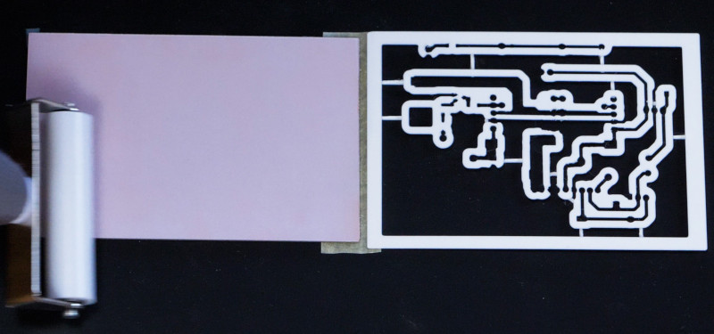
But if you’re looking for the short version, the process involves taking a 2D DXF from your PCB design software, converting it into three dimensions, and printing it out. This is then placed over a copper clad board that has been coated with soldermask, and a UV light source is used to expose it. Afterwards, isopropyl alcohol can be used to wash away the unexposed mask, leaving behind your PCB design.
You’ll still need to chemically etch the board, and if you’re using through-hole components, manually drill your holes. But compared to some of the old school methods of making your own boards, it’s relatively straightforward. This technique looks like it could also hold promise for small scale production, as the stencil can be reused indefinitely.
If your 3D printer is of the resin variety, don’t worry, you can make PCBs with those as well. We’ve also seen impressive boards produced with cheap laser engravers, as well as budget CNC routers.


This seems like it is much more involved and much lower resolution than a laser-printed stencil.
…Or just drawing it in sharpie or something. Too fiddly for mass production, too many steps and too much effort for a one-off.
The cheap inkjet photo-gloss paper can print surprisingly well on a laser printer. It requires the copper be cleaned with fine steel wool, and polished with a dry paper towel. However, it is pretty easy to iron on the paper, press under a stack of books to cool, and peel off dry. We even managed 2 sided boards with 0.5mm pitch pads using PCB alignment guide holes and foil tape. However, I must admit despite Ferric Chloride etch rates will often leave a much cleaner edges on the copper.
I am glad we live in an age where we can order proper boards in a week. ;-)
Using sticker vinyl works well too. I think there is an article on here about it.
Got a laser printer for under $200?
Obviously if you throw more money at something it is generally easier with better results.
Yes, if you check google shopping you can see brother laser printers starting at euro 110. Which is about USD 110 at the moment.
Do you know any 3d printers under 200 usd though? Yeah probably since nowadays everything is cheap except gas and gas lol
You can get hp lj 1100 in working condition for 20€ around here. And toner oack for another 20 that will last You 10years of printi g stencils
‘stencil can be reused indefinitely.’
Good luck with that.
Note the large features in the example. In the real world you’d need many bridges, which will break.
This is just ‘only tool is 3d printer/everything is’ syndrome.
If you can do it with this, you can do it a resist pen.
This is a solved problem at all scales.
I’ve never etched a UV sensitive board so maybe the problem is the same.
But I have used a resist pen and the result always sucked.
By the time the etchant has completely eaten through the copper between the traces it has also started to disolve the resist pen ink resulting in thin, pitted traces.
Then you mostly likely aren’t using the etchant properly … or you are using especially thick copper foil. The etchant should be reasonably warm and the bath should be agitated (sloshing by hand works fine). I’ve used resist pens designed for the task, but have also used simple Sharpie ultra fine tip markers with good results.
I’ve used heat lamps to warm the etchant and attached muffin fans with the blades broken off one side to the bottom of the trays in order to agitate it. I think I even tried something with the door of a cd-rom drive to rock the tray back and forth.
I’ve tried both fresh bottles of Ferric Chloride and Muriatic acid with and without Hydrogen Peroxide added and with and without pre-disolving some copper in it to try to make Cupric Chloride. With the later I even added an aquarium bubbler.
It has always taken way longer than any directions ever said it should and the result has been mediocre at best.
The best results I have had have been with transfer paper applied with a laminator which I modified to get hotter. Forget about using a clothes iron. I’ve tried a couple of them and they never really get hot enough to transfer. I don’t know how anyone has ever had success with that.
My blank PCBs are a large pile of old stuff I picked up in a box at a hamfest years ago. I do scrub it good and shiny before I try to use it but I have no idea what the thickness of the copper is. Maybe that is my problem?
I gave up years ago. My plan now is to finish a list (that exists in my head) of upgrades to my 3d printer then switch gears to a new project and build a CNC router whose main purpose will be to route PCBs.
Yes, it is possible that the older boards have thicker copper.
CNC routing will work, of course, but the resolution won’t be great and I don’t see how you avoid burrs since copper is so soft. Hope it works out for you.
I work at a school and have been etching PCBs with students for 20 years using ammonium persulphate and it works just fine. We heat the solution on a heatplate and agitate while etching (and have a fume hood for the toxic fumes) but on average, a board would be done in 5-10 minutes. We have gone from contact printing artwork onto a photographic film (high-contrast kodak/ilfocrome) in a darkroom to simply printing directly onto trace paper which is transparent enough for the UV box. We used to expose onto negative resist precoated boards then develop with sodium carbonate from memory to using kinsten positive resist stuff and develop using sodium metasilicate. I have always found the boards are good to 10mil detail or so… That was always sufficient for us 99% of the time.
I’ve experimented quite a bit with routing PCB’s on a CNC and I’m not doing it anymore unless absolutely necessary. For small boards and thick traces it’s fine, but anything more complex or doing fine traces the fun factor goes quickly down. 12 mil (0.3mm) is doable with aliexpress grade vbits (well, 80% of the bits that arrive in a package are not suitable based on my experience)
Anyway, haven’t really done any etching but I got to wonder if it’s an old pile of PCB I imagine there can be a tough copper oxide layer on top which could result to unreliable etching performance? A fine sandpaper might do wonders followed by a soap wash and a rinse to remove any remaining grease?
Truth is, I haven’t used a resist pen in 30+ years. Those worked OK, granting I was drawing features as big as the examples in TFA. Mostly the etchant seeped under the edges.
Similar experience, just print a master on a laser printer, the ferrous in the Laser powder is quite UV opaque. Used it very reliably with precoated Kinston positive PCB time and time again. The UV light box was a major contributor to quality and reliability.
Well done.
Agree. I designed a simple resist pen holder for my Prusa MK3S+ and it works like a charm. I don’t even use a DXF file … I draw the pattern in PowerPoint, save it as jpg, convert the JPG to SVG, import it into OpenSCAD to linear_extrude the pattern a mm or so, then save it as STL for slicing to gcode. Yeah, that’s pretty clumsy but I don’t have to mess with DXF and subsequent conversions.
In any case, using the resist pen (I’ve even used ultra fine tip Sharpies) gives me PCB patterns with plenty of detail.
Interesting! That would deserve an article here! Have you documented this process somewhere already?
Used laser printers are dirt cheap nowdays. If you are afraid of radioactive toner particles then you could store one outside, in a hermetic box.
I don’t like the bridges.
I am wondering if the stencil could be printed on a thin, flat UV-transparent surface and left attached to make the bridges unnecessary. Just clip the material to the bed, print, un-clip and place it over the board.
What to use? It has to be thin so as not to cause a parallax issue. People use overhead transparency material for UV curing PCBs right?
Then again, as I think that process through it starts to make more sense just to turn the printer into a plotter with a pen mount and draw on a transparency.
Aren’t there transparencies that are meant to go into a paper printer? And wouldn’t that be easier plus have better resolution?
Ok, I’m done now. I didn’t start this to knock the idea, just to suggest a possible improvement Then one thought lead to another, lead away from 3d printing. Sorry.
From the video it looks like this worked out well for the YouTube author so.. good job!
This is way overengineering it. Just print directly onto glass, flip it upside down so that the plastic stencil traces contact the PCB.
Exactly. If someone insists upon 3D printing a mask for UV film this is the way to do it.
Or cut out the middleman and print directly onto the PCB, using it as the build plate.
Or cut out the FDM printer entirely and use the UV printing capability of a resin printer to expose the photoresist directly. The newest 8K printers have a pixel size of 22 micron or 0.9 mils, which should be way more than you need for even the smallest surface mount parts.
I know someone who does this. Makes impressive quality boards if you expose it evenly
Even the cheapest Ink printer has better resolution than a 3d printer, transparent film for Inkjet is cheap too.
Why would you want to use a 3d printer?
Very weird.
agreed, I am baffled on why I would ever want to do this, even a 25 year old printer could whip out a dozen copies on transparency film before the 3d printer even warmed up
… and they are reusable too
… and can at least do good enough for QFP/QFN packages
… and not have to worry about parallax effect creating shadows
just weird
They were so preoccupied with whether or not they could, they didn’t stop to think if they should.
I have even used plain 80gsm white office paper as stencil for uv sensitized boards. Worked okish (forgot to put a piece of glass on top most of the time..)
If I was going to use my 3D printer to make a PCB I would just use a blank board on my print bed, lay down a layer or two direct on the copper, then etch that.
We tried using a couple of layers at work to act as the mask directly to copper clad boards. Unfortunately we couldn’t get good adhesion. Maybe we didn’t polish enough or picked the right material to print but found the temp change as the board and print cooled meant it pealed off too easily also the definition wasn’t enough for us.
We ended up printing ink directly to pcb to act as mask then etch in ferricC, it does need to be warmed or takes ages also needs agitation like bubbles, perhaps a fish tank aerator might help. If we forget to turn our bubbles on after 10 mins still no etch.
I had wondered about using a paint sprayer with a small acrylic or 3d printed box to house the pcb, with a pipe to recycle the etchant. Might be able to get the etching process down to 2-3mins that way. It would need to be a wide nozzle so it covered the pcb.
Kind of just echoing everyone else on this, it looks like, but I’m struggling to find a legitimate use case for this. Short of simply not having a regular inkjet/laser printer, I can’t come up with any reason you’d prefer to do it this way. The resolution’s worse, it takes way longer, it’s (possibly) more expensive, it’s fragile.
The ONLY thing I can think of is that it’s guaranteed to be opaque. A lot of cheap inkjets or lasers don’t or can’t put on enough ink to produce enough contrast, and inkjets may even leave pinholes here and there. Even then, I’ve gotten around that by printing the artwork twice and taping the two together. Bit fiddly to get them aligned, but it works fine down to 15 mil or better on 1oz copper.
Thought it was going to be something like this: https://github.com/Andrew-Dickinson/photonic-etcher
Which is a much cleaner technique
That is rad! Nice workflow!
best way to do this with an FDM printer is to forego the hotend entirely and add a spring-loaded, sharp nail that scrapes on the board. simply get a new pcb, paint it entirely with one or two layers of permanent marker (more layers might make it chip away – just 1 will usually suffice) then use Flatcam or something less horrible to make gcode for the printer. You’ll have the unwanted copper areas ready for etching with ferric chloride.
I’ve been able to make 0.2mm traces with this method, and soldered a QFN48 0.4 with it.
This would have been more worth of an article than the 3dprinter thing above.
No because we’ve already seen that article here a few times. It’s just been a while.
This is a silly idea. BUT. Using the heated bed of the 3D printer to bake the soldermask ink/paint is something I havn’t thought of before, and could be a jolly good idea. That stuff is a real PITA to work with wet and is supposed to be carefully oven dried and is quite temperature sensitive I understand, so, if sitting on a heated bed works…. that’s worth some internet points.
I tried etching / agitating on the heated bed for a while. It ran a heat up, go-forwards-go-backwards gcode for like 10000 reps. Board in a tupperware so it doesn’t spill or fume, naturally.
You still have to watch over it to tell when it’s done, so it’s not really all that much better than floating the same tupperware in a sink full of warm water and sloshing it around manually.
I’ve etched boards on my workbench and noticed that metal tools hanging over from the shelf above started to tarnish from the corrosive fumes. That makes me kind of resistant towards trying it on the bed of my printer!
You probably didn’t used an airtight container, then.
I’ve seen BigClive do his etching in a (cheap) Ziploc bag (clone). Folded over at the end with an extra clip for spill protection.
However I have no idea how well that works.
Only etched a PCB once in my life. In the 80s. And we did it in an old pot (the ones that are glass coated on the in inside, dunno the English term for that, though). And I’m also pretty sure we used hydrochloric acid.
But using an old or crappy 3D printer (have seen Ender 3 clones around 150€) and just using the heated bed for rocking the solution has potential in my eyes. Technically you could modify Marlin to a point that it only uses one axis and the heated bed and throw out everything else. Or keep the Z axis and use it to press a webcam in regular intervalls against the Ziploc to (remotely) check if etching is done.
Unfortunately the quality of this is worse than just attaching a marker to the print head and drawing on the PCB. Or attaching a dremel extension to the 3d printer.
and the link https://www.instructables.com/Printing-Custom-Circuit-Boards-With-a-3D-Printer/
Why can’t you just print right on the copper surface, then peel it off after etching?
Pcb2gcode your gerbers and use a CNC with a small milling bit, you can have an isolation routed, drilled (any diameter), and edge cut (arbitrary shape) single sided PCB in 20 minutes. A 3d printer is clearly the wrong tool for the job here.
What if you just 3D printed an inverted design directly on a piece of glass? Then you would flip it over onto your PCB and UV cure through the glass. This assumes that your 3D filament will stick to the glass, IDK, but some printers do have glass beds so it seems possible.
would be really bad for fine pitch. also it would have thickness so unless you use a collimating lens, you’ll have shadows
Pretty useless, use the correct tool for the job, this is like screwing bolts with a hammer.
I understand this might be a bad idea but I was wondering if anyone has tried to print and pause layers laying the wire into channels and having it come out where it prints pin holes?
It could even 3D encapsulate the header pin and then solder could be added to connect them on the back side of the holes.
I was just thinking a simpler and cheaper way other than getting the copper plate and solder mask.
Let me know what you think. I’m going to try it out.