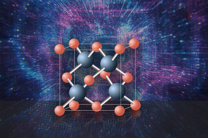
Silicon has had a long run as the king of semiconductors, and why not? It’s plentiful and works well. However, working well and working ideally are two different things. In particular, electrons flow better than holes through the material. Silicon also is a poor heat conductor as we’ve all noticed when working with high-speed or high-power electronics. Researchers at MIT, the University of Houston, and other institutions are proposing cubic boron arsenide to overcome these limitations.
According to researchers, this material is a superior semiconductor and, possibly, the best possible semiconductor. Unfortunately, the material isn’t nearly as common as silicon. Labs have created small amounts of the material and there is still a problem with fabricating uniform samples.
Early experiments show the material has very high mobility for electrons and holes along with thermal conductivity almost ten times greater than that of silicon. It also has a good bandgap, making it very attractive as a semiconductor material. In fact, only diamond and isotopically enriched cubic boron nitride have better thermal conductivity.
However, there are still unknowns about how to use the material in practical devices. Long-term stability tests are as lacking. So maybe it will wipe out silicon or maybe it won’t. Time will tell.
We are always on the lookout for the next big semiconductor material. However, we suspect this tech will be out of reach to the home semiconductor fab, at least for a little while.


GaN
Great semiconductor, rather expensive, and used when needed. This could be even greater, even more expensive, and used when GaN still won’t cut it.
All this to say, this new semiconductor may become the future of compact power management components. Silicon will be with us while electricity is still metered.
Extremely difficult to melt grow a GaN substrate, requires temperatures >1600˚C and pressures >45,000
atmospheres, and is really really really really slow. Much as I would love it to take over from Silicon yesterday, with Silicon there is 68 years of knowledge and problems that are already solved. There will NEVER be a perfect pull ( https://computerhistory.org/blog/patricias-perfect-pull/ ) of a GaN substrate, unless there is an amazing breakthrough (You are probably talking about a Haber-Bosch process level of amazing breakthrough).
GaN is fantastic but there is still decades of work needed for a GaN substrate material, it is currently produced by Epitaxy Growth – by depositing a thin layer (0.5 to 20 microns) on a foreign substrate.
Why in the world would you want GaN to take over from silicon? It’s not like it’s just flat out better straight across the board. GaN’s main benefit comes from being able to shove lots of current efficiently and quickly: power stages, amplifiers, etc. But once you get to the signal processing stage and all you care about is shuttling information, a wide bandgap doesn’t help.
Honestly it’s kindof a similar issue with BAs here – its real advantage is the 10x higher thermal conductivity, which is why there’s been research into heterogenous structures (GaN to move the electrons, BAs to move the heat).
Since about 2005* clock rates have effectively flat lined because there is no cheap and easy way to extract heat faster than the silicon would become lava, so 10x higher thermal conductivity might help with all the problems constrained by Amdahl’s law.
* https://github.com/karlrupp/microprocessor-trend-data
It’s not heat that’s the limit. The gate oxide thickness limit was reached around the time of ’22nm’. That’s also when switching voltage hit the ~1v floor, and the 5GHz practical ceiling, both stemming from that gate oxide thickness.
@psuedonymous
Look at slide 8 of an old Intel slide https://pdfs.semanticscholar.org/6a82/1a3329a60def23235c75b152055c36d40437.pdf
We are both describing the same same end result, power density can not be reduced because there is a lower limit for the voltage required for the analogue circuitry to function. Everything remaining on the table that could be could be dialled up for faster switching will generate additional heat. Heat may not be the ultimate limiting factor, but it is the failure mode. If you could remove the heat the chip would not melt, and you could gain extra clock cycles even with greater power usage.
Omega particle
Upp, bupp, bupp bupp. Bad idea.
Still waiting on the decade+ “carbon nanotubes” in processors to boost performance to the tune of an order of magnitude. Still heard nothinf about that yet.
Wake me up when i can buy one to play minecraft on.
“We are always on the lookout for the next big semiconductor material. However, we suspect this tech will be out of reach to the home semiconductor fab, at least for a little while.”
Still have supply chain problems, just with a new material.
+1 where’s my silicon on saphire, diamond on saphire etc. (though SiC use is finally expanding I guess)
What happens when the magic smoke escapes and it loaded with arsenic!
Haha I’m curious as well!
Having a material that mostly consists out of a material that more or less is banned for use in almost anything makes it a large uphill battle to market.
It is partly a similar story for Gallium Arsenide based semiconductors already. And these are somewhat rare. Even for applications where they would be advantageous.
Though, arsenic is used as an N type dopant in a lot of semiconductors. However, a dopant doesn’t need to be particularly concentrated, and where it is used there isn’t a lot of volume of it either. In the end, it is practically like it isn’t there. There is likely more arsenic in a tree than a CPU for a given volume.
But this obviously wouldn’t be the case for a bulk material consisting of ~50% arsenic.
Gallium arsenide had its day, for 20 years every cell phone had a few square mm of GaAs die in it; most of the radio circuitry was GaAs. Many phones still do have it in the RF power amplifiers.
Just rework the old RAID slogan, “BUGS KILL DEAD!”
The earth is made mostly of iron, oxygen and silicon, so nothing much is going to be as common as silicon. But who cares, it’s going to be used in relatively tiny amounts. The processing effort will dwarf the effort in finding material.
Don’t forget aluminum.
Please, can we not go back to Al?
Silicon Carbide is becoming more common in power electronics.
But for me it’s quite simple. I have no aspirations to go make my own semiconductors, so I just limit myself to what I can buy, and datasheets usually don’t even mention what the things are made off.
“and datasheets usually don’t even mention what the things are made off.”
That’s because if the device isn’t in one of the markets where other semiconductors are used, it’s all silicon. RF amplifiers, power devices, etc. all will list manufacturing processes in the datasheet, be it silicon, GaN, GaAs, InGaP, SiGe, etc.
I mean, go to Mouser’s RF amplifier selection and the manufacturing technology’s right in the sort table.
Yeah I know someone who helps design silicon carbide for high current/voltage power electronics. No idea how the cost stacks up but the original article implies that this new stuff might be a big improvement if economics & production work out.
Neat stuff. Always comes down to ease of mass production and/or cost. How many times have we heard of new materials that are going to revolutionize batteries, circuits, etc. But fall my wayside, because they can’t produce it economically at larger scale. I always thought Carbon Graphine was going to be ‘the’ magical material for example… As we know Carbon is quite ‘common’ on the planet (even has some worry warts worried about it being so common)…. But here we are years later…. not much if any progress on that front.
When I was working in gallium arsenide, the joke was “GaAs is the semiconductor of the future, and it always will be.”
ISTR, Seymour Cray tried using GaAs memory in his Cray 3, and wasn’t able to complete it.
?
Shortly thereafter multiple processor machines made headway.
All of the comments here in this thread about Gallium Arsenide seem to miss the fact that it is pervasive in LEDs.
Indeed. That’s one of the rare places where there are fundamental physical constraints preventing silicon from ever making inroads. The kernel of my statement about it being the semiconductor of the future is that various silicon, SiGe, and GaN processes are always nipping at the heels of GaAs. In the ’90s it was RF receivers, GaAs MESFET was the superior technology until CMOS got good enough and the baseband IC could start pulling in the mixers and LNAs, becoming a radio IC and killing off the discrete receive business. Then it was GaAs HBT (heterojunction bipolar transistors) which were the bees’ knees for PAs. They lasted for half a decade for so before being displaced in the WLAN space by SiGe and later CMOS. SiGe could never get there for cellular PAs, and GaN is having difficulty, so GaAs HBT and PHEMT (pseudomorphic high electron mobility transistor) is still the dominant tech there. On the synthesis and optical sides, GaAs was used almost exclusively in the ’90s and into the 2000s, but CMOS/BiCMOS has made great inroads there. Now we’re integrating 30 GHz VCOs on silicon die which would’ve been unimaginable outside the “exotic” materials space a couple of decades ago. That wheel keeps on turning.