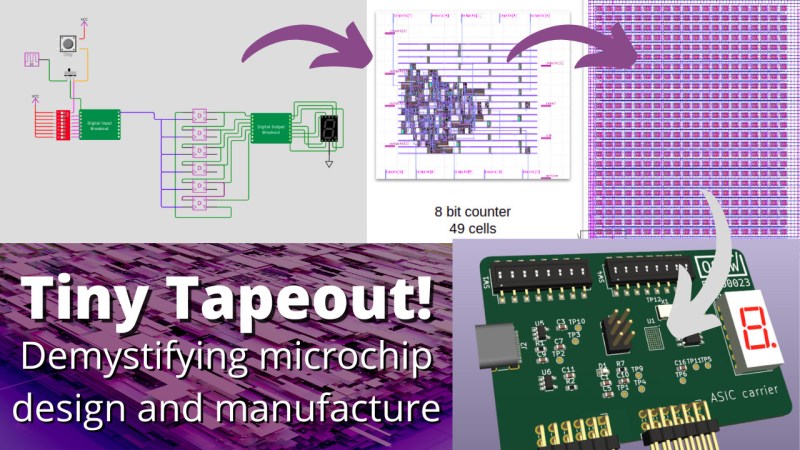
When hackers found and developed ways to order PCBs on the cheap, it revolutionized the way we create. Accessible 3D printing brought us entire new areas to create things. [Matt Venn] is one of the people at the forefront of hackers designing our own silicon, and we’ve covered plenty of his research over the years. His latest effort to involve the hacker community, TinyTapeout, makes chip design accessible to newcomers – the bar is as low as arranging logic gates on a web browser page.
For this, [Matt] worked with people like [Uri Shaked] of Wokwi fame, [Sylvain “tnt” Munaut], [jix], and a few others. Together, they created all the tooling necessary, and most importantly, a pipeline where your logic gate-based design in Wokwi gets compiled into a block ready to be put into silicon, with even simulations and compile-time verification for common mistakes. As a result, the design process is remarkably straightforward, to the point where a 9-year-old kid can do it. If you wanted, you could submit your Verilog, too!
The first round of TinyTapeout had a deadline in the first days of September and brought 152 entries together – just in time for an Efabless shuttle submission. All of these designs were put on a single instance of a chip, that will be fabbed in quantity, tested, soldered onto breakouts, and mailed out to individual participants. In this way, everyone will be getting everyone’s design, but thanks to the on-chip muxing hardware, they’re able to switch between designs using on-breakout DIP switches.
More after the break…
 The constraints are simple. You get eight digital inputs, eight digital outputs, and there are 200 gates at your disposal. What could you build with this? For a start, a BCD to 7-segment decoder, a UART transmitter, or even a full 4-bit CPU – or maybe, a Wolf, Sheep, and Cabbage game! After the first round of submissions ended, [Matt] has asked people to compile information about their designs – here’s a PDF datasheet with over 30 various designs for you to marvel at, from Hello World ones to CPUs, a variety of circuits with practical or educational purposes.
At the moment, [Matt] is already planning the next TinyTapeout run. If you have a project idea asking to be brought into cold hard logic gates, sign up for the mailing list and you won’t miss news about the next TinyTapeout deadline. The Wokwi template is already open for your experimenting purposes, all that’s left is for the submission form to go open. If you have any questions, the FAQ is quite helpful!
Of course, such projects don’t happen out of nowhere – for a few years, [Matt] has been bringing us hackers teachings on how to get into chip design. We’ve hosted his Zero to ASIC workshop in 2020, the OpenMPW progress story at Remoticon 2021, and just this year, a HackChat on open-source ASICs. TinyTapeout reminds us of the story of how OSHPark was founded – a bunch of people pooling together to order their PCBs, and just like back then, we foresee some fun additions to a regular hacker’s toolkit.


“using on-breakout DIP switches”
On-board breakout DIP switches?
on the breakout board, shortened to on-breakout.
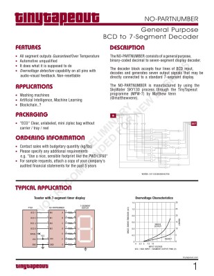
A BCD to 7 segment IC is pointless. It falls into the category of things that can be done using a 256 Bytes ROM.
The limitations are;
8 pins input
8 pins output
~100 khz max
~200 gates max
Without doing any math, you can already know there is no way to have more than 200 bits of internal memory. Thats 25 bytes.
Anyways, I might try to make a very small programable FPGA, using those restrictions. Just for fun. With 200 gate limit, I think I can make one that features ~4 Logic Blocks.
Lets see how many Logic Blocks anyone can push on those restrictions.
Hey, this FPGA made it on to TT01: https://github.com/gatecat/tinytapeout-fpga-test
It’s far from pointless, this project has immense educational value for participants. Someone’s going to have their BCD-7segment decoder fabbed, and they’ll be able to look through the Verilog, the chip 3D renders, study the very real thing they’ve built down to the gate level, and with this understanding, will be able to proceed further in ASIC world if they so choose. It’s like with a kid building a LED flasher circuit, tweaking the parameters, getting some real educational value out of probing it and then going on to study electronics – you wouldn’t compare that to a skilled engineer using a LM3909.
Completly agree with you on the “educational perspective”. I dont argue that.
But imagine if we try to push this oportunity to the limit, and figure out the max we can get from those limitations. I aint complaining about those limitations. I am on my “Apollo 13 mode”, trying to figure out how to hack something big out of something small. For fun =)
Kinda related: https://youtu.be/MBT1OK6VAIU
oh, I get you! I was addressing the “BCD-7seg IC is pointless”, in this case, even such a small project isn’t. I also quite like your “get more out of it” approach, and would like to see how your FPGA project exploration goes!
At the moment I can get it to do a 1 LUT. Haters would claim it is just a 4 bit SRAM chip.
I agree there can be educational value in something like this, but at least in the first iteration the result is rather disappointing in that regard.
Since the whole manufacturing process itself was abstracted away, the only thing you could really learn from this project would be in the differences between simulation and reality. Timings, hazards and such. But most designs handed in are very trivial and far from using even half of the 200 gates. Too many are even identical. Many don’t need any clock at all, and if they do, they’re limited to the 12.5 kHz of the surrounding chain logic so you can’t even really test the limits of your design.
I think quite some opportunities were lost, especially considering the cost. The biggest one being not bringing people who had the same idea together so they can join forces on a bigger design (why not let them pay for a 400/600/800 gate design together?), learn from each other etc.
Looking forward to round 2.
Thanks for the feedback!
We do want to expose more of the manufacturing process. At the moment the idea is this will be done via emails after someone submits a design. Maybe a virtual tour of skywater’s foundry.
We also want to show more of what’s happening before the standard cell, so looking at how mosfets work etc.
This is still very much a work in progress. There’s lots of room and ideas to improve. The first hurdle is seeing if the project is really viable, then move onto adding features.
I think it’s amazing and don’t understand people who are poopooing you for it. I guess they mastered chip fab in 4th grade and think everyone else should be designing M1 chips like them.
Every project you’ve done has been about reaching and teaching advanced concepts to beginners and I’m grateful for that. Sometimes I wonder why people enjoy this site when they make the same comments on every project, “this is just ____. You can get it on Amazon.” Glad to see a Hacker on HAD and thanks for helping me learn about things I didn’t have the privilege of learning as a kid.
Sometimes the point of an exercise is the creativity that comes from the constraints of the situation.
7446, 7447, 7448 BCD to 7 segment ICs.
Soo.. someone made a 74HC47? :)
I really like the idea. But that the designs can just run at about 12.5 kHz max is a big limitation. It means it is mostly “playing around”. At least I would be much more motivated to design something with it if it would allow some practical application where a MCU based solution wouldn’t always be running circles around the ASIC.
Maybe reduce the amount of possible designs from 500 to something lower and use the space for some deep mux stages instead of a scan chain.
If it ran faster, that would be nice. The ability to daisy-chain modules would be good, too- but might be tricky to implement.
My idea for a variant would include a decent ADC and DAC, along with a high speed internal bus. Users could choose from input pins, or the ADC data. Output to DAC or output pins.
long term we really want an analog version. Shared ADC/DAC/serial etc has already been suggested and could be added if there’s enough interest / time / energy etc.
All I want is the possibility for analog designs (and at least 1MHz clocking) so I can reimplement the MOS6581
I’m going out on a limb here, but maybe playing around is the point?
I agree the frequency limitation is a bit of a bummer, and I thought it could be circumvented by adding a ring-oscillator, if a higher but not precise frequency need to be generated. I saw that some ring oscillators were implemented in previous TinyTapeouts, and possibly can be re-used. Unfortunately, this would steal some further gates to the already meager ~1000 count that can fit the TinyTapeout.
Still, I decided not to pursue this road, because I am afraid it might be complicated to get it through the backend flow (ie not sure how the constraints are specified in this case).
Perhaps one day one of the 500 TT slots could be used to implement a digital PLL that could provide a higher clock, if needed: the IOs would still be limited, but internally the HW could run much faster. This configuration could make sense for instance for a simple HW accelerator.
I love the idea of being able to design my own ASIC for my own use….
However, looks it’s $100 for 1 part mounted on a PCB. The slow speed comes from the fact your design is accessed by going through a scan scan. Main design interface shown is a graphical schematic capture that looks painful for anything complicated…
I’m also not sure who this is targeted for. Beside the “cool, I have a chip that was fabricated for me”, I would argue a beginner would learn much more about digital design by using a cpld or a fpga. The front end GUI looks like it can easily be retargeted for a simple cpld since you get verilog code. $100 buys you a lot of development boards.
Anyone who is more technically knowledgeable would absolutely be turned off by the limitations…
I applaud the team for trying to get something that cost a lot of money into a more accessible form. I’m just not sure how useful this is, as it is now.
quick comment – afaiu the $100 is for the breakout and reflowing the chip onto it specifically, so, getting the ready-to-go package instead of WLSCP. I’ll go and confirm this though.
Thanks for the feedback!
Target audience is high school, hobbyists, undergrad, professionals having fun.
Yes we are sacrificing speed and area to get the price down. 1 chip run is $10k.
The GUI is for people who are totally new to digital design. We also support HDLs for applications.
And take a look at these for some technically knowledgeable people who absolutely were not turned off by the limitations! In fact a few people mentioned that the limitations helped them.
https://tinytapeout.com/runs/tt01/#hdl-projects
And yes, I agree this is kind of a novelty at the moment. It would be much faster and easier to learn digital design with an FPGA. We hope to support mixed signal in the future which I think could be extremely useful.
Did anyone lodge a 555 timer?
I would hope so. Would make a very useful reference design if nothing else. If not this time round …. get it done next time!
Nice work. If flip-flops can be constructed out of this and number of gates is increased, it might be possible to build a fully functional microcontroller of sorts.
one question, is possible make a 4-bit processor from beacon https://hackaday.io/project/182568-badge-for-2020-supercon-years-of-lockdown ?
I think so. The register width is only 4 bits – so the RF is only about 8 bytes. The decoder and execution units are also small. Try it out.
It’s not pointless if you want to learn some basic digital logic gates, karnaugh map, and design. There are better ways, but it’s a classic one and no reason to say it’s “pointless”.
If you are a student, and can’t either afford $100 for a custom designed ic, or if the oportunity has already expired, you can do this;
https://youtu.be/BA12Z7gQ4P0
A BCD to 7 segment IC falls into the category of combinational logic. The benefits, other than being cheaper and faster, is that you may reuse the same EEPROM to upload your new combinational logic ic.
If you are a student, and you wish to learn more about digital logic, you can check out the former youtube videos. No need to expend $100 on a single, one time use, IC.
Cheers
yes, its for beginners – but when you like (and have the required skills) you could design your own (analog) stdcells. Hurry up, the deadline for the next (up to 500) designs is near : https://tinytapeout.com/runs/tt02/
Just my somewhat related personal rant;
https://www.reddit.com/r/AskElectronics/comments/k4s6be/why_cant_i_get_an_fpga_in_a_dip_package/
I have a personal need for a DIP 16 PIN FPGA, so I could emulate just about any random 7400 series IC. Considering the current chip outage scenario, is logical that people are looking for alternatives, even if they are expensive, because there is no other choice.
If the goal is to create an educational tool, then what better tool than an arbitrary re-programable breadboard friendly 16 PIN DIP FPGA.
Currently there is NO-ONE providing this solution. So this might be a business oportunity to some, and a blessing for consumers in need for some rare/old ic.
Thanks for reading
SLG46826V-DIP, 2$ fully mounted on a DIP20-sized breakout. Not quite an FPGA though. Easy to program over naked i2c, so no need to buy their programming boards if you don’t want to. 5V TTL compatible. Bitstream fully documented in the datasheet if you don’t want to use their tools (which are however pretty good and available for Linux too).
I use them for all sorts of stuff, especially on breadboards where I’m currently lacking the exact 74xx chip I need.
Is there some documentation to go with that other than just a pin out diagram?
Yes. I spent 30 seconds searching Google from my phone. It would have taken you less time than your comment did to do the same.
DIP carrier board (includes the chip, but the datasheet is just about the carrier board): https://www.farnell.com/datasheets/2875116.pdf
The chip itself: https://www.farnell.com/datasheets/2803600.pdf
Answer: there’s no money in low density footprint FPGAs.
Volume customers won’t pay the FPGA premium for a tiny bit of glue or slow control logic. 74 series logic and microcontrollers are a much cheaper alternative to many applications where an FPGA could be used.
Just as with microcontrollers that have mostly given up DIP packaging, there are plenty of hobbyist FPGA boards in a DIP form factor. TinyFPGA, UPDuino, Arduino MKR Vidor 4000, and the Lattice ICEStick are popular and relatively inexpensive FPGA boards that can be used in a breadboard.
As for using FPGAs for replacing rare ICs, that’s being done already. Most of the chips on a C64 have modern replacements made from FPGAs, CPLDs, PALs, or microcontrollers. On a more macro level, there are many microcontroller and SBC projects that emulate larger chunks of vintage systems, like UniBone which can emulate any QBUS or UNIBUS board in a vintage PDP or VAX system, or TIPI which uses a Raspberry Pi to emulate peripherals on a TI 99/4a expansion bus.
Thats my entire point here. I cant get a 16 pin DIP FPGA anywhere, but I can submit a simple design and get one for $100.00
=)
Don’t count out Atmel/Microchip, especially the ATF chips. The design tools are a bit old, but I have made C64 PLA and “Wrapper chip” to use 6502 CPU instead of the 7501/8501 CPU for the plus 4. SMD parts can be mounted on breakout boards to be DIP. You really don’t need an FPGA for random 7400 series logic gates….
I love the idea and I am waiting for an analog version. Integration has an enormous potential för analog circuits when you need to rely on matcher transistors. You could make custom TIAs, current source drivers, amplifiers, if you could have an IC block for a op-amp custom analog computers to implement simple neural networks.
Totally amazing, love this! :-)
Now tell me how go from this to an asic with 112G PAM-4 transcievers? because right now no one will even talk to me for less than $25M and 3 years dev time.
Well, there are some alternatives;
https://www.thefoa.org/tech/sciproj.htm
It saddens me that i have a plasma Etch too sitting here next to me and i can’t help out with projects like these. I’m all for building anything because the gains in knowledge surpass the limitations of the end product. It’s just too bad i don’t have access to litho and everything else needed to let people use my Etch Chambers.