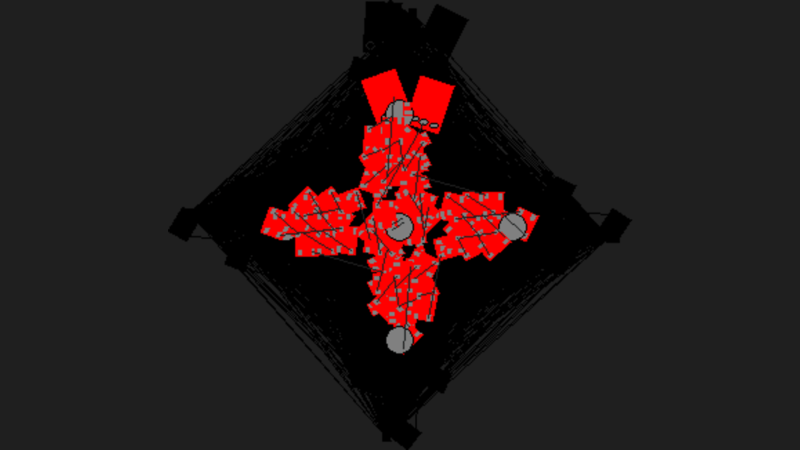
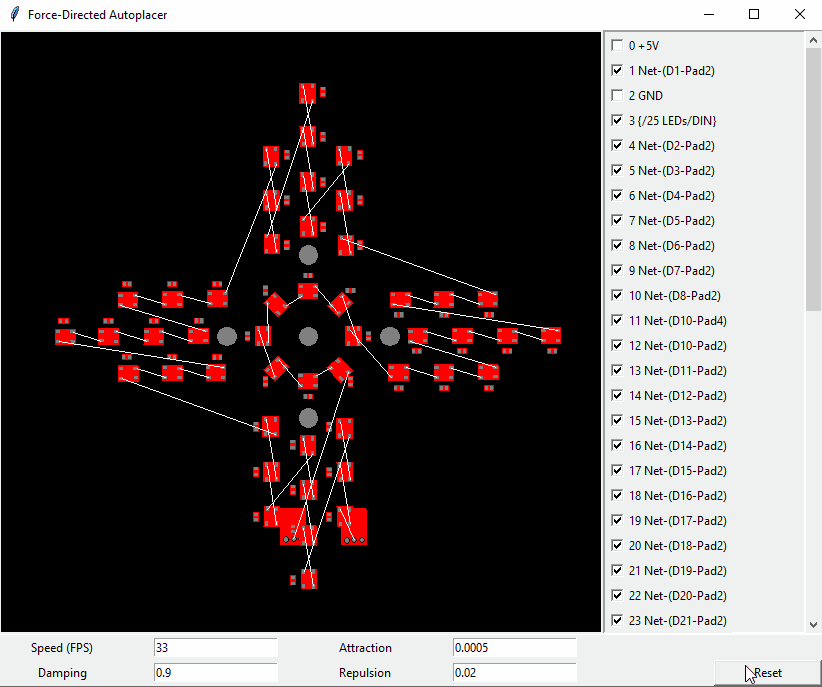
[Jarrett] recently stumbled upon a class of drawing algorithms called force-directed graphs, which artificially apply forces to the elements. The final graph is then generated by applying the laws of physics and letting the system reach equilibrium. This can often result in a pleasing presentation of things like mind maps and other diagrams without having to hand-place everything. He realized that this approach almost mimics the way he places components when doing a PCB layout. Out of curiosity or intense boredom, we’re not sure which, he decided to implement this in a tool that interacts with KiCad ( see animated GIF below the break ).
He has to ignore certain nets such as power and ground rails, because they distort the result. This simulation treats the nets as springs, and the center of each footprint behaves a charged particle. [Jarrett] added a twist, literally, to the usual implementations — each net pulls on its pin, not the part center, and therefore the chips will both rotate and be pushed around as the system stabilizes.
The results are sometimes quite striking. Useful? Dubious, but maybe!
The project code is up on GitHub, but is very experimental and he is unlikely to carry it further. Among the missing features, the Python code must be tweaked for each different netlist files and other parameters, and there is no way to feed the result back into KiCad. But this is enough for [Jarrett], who only set out to see if the concept was possible. The code is available if anyone wants to try their hand at taking this to the next level.


I had an idea for something just like this about a decade ago. It would be great for auto placement of parts for pcb layout. Unfortunately i didn’t have an open source cad package at the time so I just abandoned the idea.
Wow – the fact that you had an idea but done nothing about it except write a comment on an article about someone who did. Imagine how bad it would feel if it had been invention of the electric light bulb?
I feel sorry for those who have sufficiently few ideas to have the time to act on then all.
Did you even think before you typed?
Light bulbs predate online forums by quite a bit and ergo comment sections. Therefore this scenario is impossible.
Also seems a bit snarky.
I had bigger fish to fry at the time. As someone who designed HARDWARE for a living I didn’t have the luxury of dropping everything and creating PCB software from scratch. Light bulbs are rather simple to design/invent in comparison to wireless communication systems.
Haha same! But then to fit 3d objects in another shape (aka 3d bin packing). The idea was to take your objects, throw them in a box (or other shape you need) and just shake the box until you reach equilibrium/optimal space use. Can obviously also be used for sorting/filtering by granular convection/’gravity’. I tried to do this in Openframeworks but never got much past the example files: https://github.com/dennisdebel/pluriform-3d-bin-packing
Interesting. The animations show how the tension in the springs wants to reduce the length of the connections. I wonder what would happen if attraction between ICs was added, to keep them packed together. Or repulsion from the edges to keep them inside some frame.
From the animation, it appears the nets are simply pulled to a minimum length, which isn’t directly useful (from a layout perspective, anyway). The animation also appears to show components with only two connections… all circuits like that will pull themselves into a circle, so I don’t think this was a particularly useful display for the idea.
It would be more interesting to see a real circuit (say, a micro with associated components) fold itself. Power and ground nets would need to be included, though, particularly if power is more than a necessary evil (e.g., what about a motor driver where the power path matters?). If one could link a net’s rules to the spring’s strength (e.g., a high-power FET drain that needs 100mils of copper to the next FET’s source), then we might see some potentially useful layout clustering.
Maybe you could add some dummy “copper pad” components whenever the length of the connection exceeded a certain length, where the size of the copper pad was proportional to power requirements of the connection. This might help with ensuring there is enough room for the routing between the components.