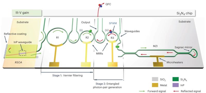
As the world of computing and communication draws ever closer to a quantum future, researchers are faced with many of the similar challenges encountered with classical computing and the associated semiconductor hurdles. For the use of entangled photon pairs, for example, it was already possible to perform the entanglement using miniaturized photonic structures, but these still required a bulky external laser source. In a recently demonstrated first, a team of researchers have created a fully on-chip integrated laser source with photonic circuitry that can perform all of these tasks without external modules.
In their paper published in Nature Photonics, Hatam Mahmudlu and colleagues cover the process in detail. Key to this achievement was finding a way to integrate the laser and photonics side into a single, hybric chip while overcoming the (refractive) mismatch between the InP optical amplifier and Si3N4 waveguide feedback circuit. The appeal of photon-based quantum entanglement should be obvious when one considers the relatively stable nature of these pairs and their compatibility with existing optical (fiber) infrastructure. What was missing previously was an economical and compact way to create these pairs outside of a laboratory setup. Assuming that the described approach can be scaled up for mass-production, it may just make quantum communications a realistic option outside of government organizations.


This seems a very important achievement. No more scientist with laser-protection googles and a complex optical apparatus on a peg board. All solid-state.
You´re right, if this can be scaled, it will be a game changer.
I mean, this will not come to a surprise to you, but a Nature photonics article demonstrating a working device doesn’t happen overnight – photonic ICs have been a research topic for 1.5 decades or so now, and in production for commercial photonic applications for a few years (think: >> 100 Gb/s optical links with an integrating package containing ADCs, DACs, lasers and modulators).
So, the difference here is really, at least according to the paper’s abstract, the successful integration of the excitation laser on the chip – and that’s been available quite a while for non-research ICs. Though I don’t know whether the specific type of laser is usually integrated, but since they are talking about “telecom band”, I guess it’s probably “just” a good laser as used in one of these transceiver ICs.
It’s not the excitation laser that’s of interest, it’s the integration with other components to produce entangled photons.
“Assuming that the described approach can be scaled up for mass-production, it may just make quantum communications a realistic option outside of government organizations.”
Quantum internet skipping all the gatekeepers.
Love reading about this stuff, but this one sounds like one of those SciGen context free grammar paper generators.
There’s an easier way to create a Q-Bit. Popular Science used to talk about it in the 80’s – regarding building a multi-layer bubble-shape and holding digital date along the edge of the bubble (onion layers).
I am building a large version of this – as a test-bed for multiple technologies found here:
https://drive.google.com/drive/folders/1-3TDKlwpr2n6tQp0ypg-qxa6P_vOIytA
“published in Nature[COMMA]”
Great work by my teacher.