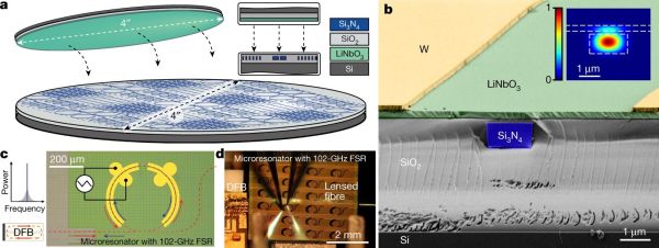
Stack of Si3N4-LiNbO3 forming the integrated laser and integrated into test setup (d). (Credit: Snigirev et al., 2023)

Fast Adjustable Lasers Using Lithium Niobate Integrated Photonics

Making lasers smaller and more capable of rapidly alternating between frequencies, while remaining within a narrow band, is an essential part of bringing down the cost of technologies such as LiDAR and optical communication. Much of the challenge here lies understandably in finding the right materials that enable a laser which incorporates all of these properties.

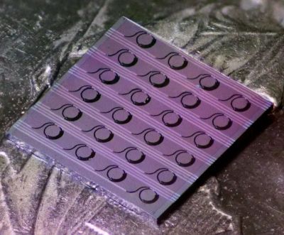
A heterogeneous Si3N4–LiNbO3 chip as used in the study. (Credit: Snigirev et al., 2023)

Here a recent study by [Viacheslav Snigirev] and colleagues (press release) demonstrates how combining the properties of lithium niobate (LiNbO3) with those of silicon nitride (Si3N4) into a hybrid (Si3N4)–LiNbO3 wafer stack allows for an InP-based laser source to be modulated in the etched photonic circuitry to achieve the desired output properties.

Much of the modulation stability is achieved through laser self-injection locking via the microresonator structures on the hybrid chip. These provide optical back reflection that forces the laser diode to resonate at a specific frequency, providing the frequency lock. What enables the fast frequency tuning is that this is determined by the applied voltage on the microresonator structure via the formed electrodes.

With a LiDAR demonstration in the paper that uses one of these hybrid circuits it is demonstrated that the direct wafer bonding approach works well, and a number of optimization suggestions are provided. As with all of these studies, they build upon years of previous research as problems are found and solutions suggested and tested. It would seem that thin-film LiNbO3 structures are now finding some very useful applications in photonics.

(Heading image: Stack of Si3N4-LiNbO3 forming the integrated laser and integrated into test setup (d). (Credit: Snigirev et al., 2023) )

Creating Lithography-Free Photonic Reprogrammable Circuits

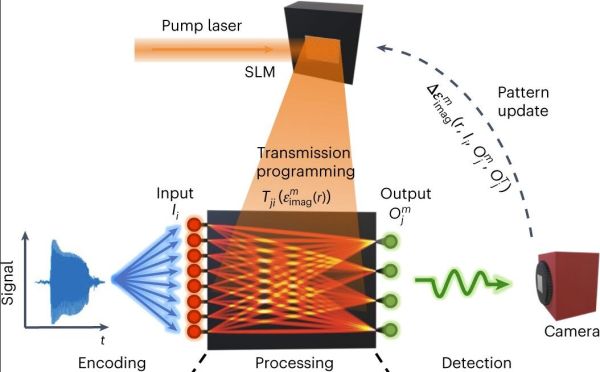
The field of photonics has seen significant advances during the past decades, to the point where it is now an integral part of high-speed, international communications. For general processing photonics is currently less common, but is the subject of significant research. Unlike most photonic circuits which are formed using patterns etched into semiconductor mask using lithography, purely light-based circuits are a tantalizing possibility. This is the focus of a recent paper (press release, ResearchGate) in Nature Photonics by [Tianwei Wu] and colleagues at the University of Pennsylvania.

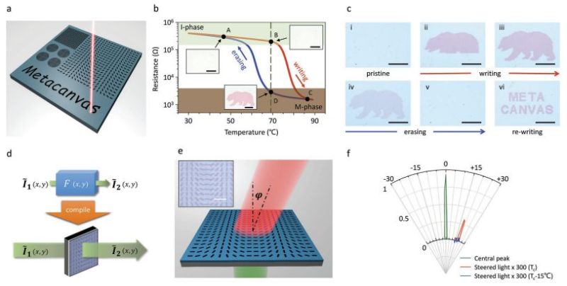
What is somewhat puzzling is that despite the lofty claims of this being ‘the first time’ that such an FPGA-like device has been created for photonics, this is far from the case, as evidenced by e.g. a 2017 paper by [Kaichen Dong] and colleagues (full  article PDF) in Advanced Materials. Here the researchers used a slab of vanadium dioxide (VO2) with a laser to heat sections to above 68 °C where the material transitions from an insulating to a metallic phase and remains that way until the temperature is lowered again. The μm-sized features that can be created in this manner allow for a wide range of photonic devices to be created.

A rewritable metacanvas. a) Schematic of laser writing different photonic operator patterns on a metacanvas. b) Temperature-dependentresistance of a VO2 film. c) Optical images from writing and erasing process on the metacanvas. . d) Diagram showing the mathematical matrix (F) is compiled onto a metacanvas in the form of a photonic operator for manipulation of light waveform (I ). e) Schematic of a metacanvas programmed as a beam steerer with a steering angle ϕ. (Credit: Dong et al., 2018)
A rewritable metacanvas. a) Schematic of laser writing different photonic operator patterns on a metacanvas. b) Temperature-dependent resistance of a VO2 film. c) Optical images from writing and erasing process on the metacanvas. . d) Diagram showing the mathematical matrix (F) is compiled onto a metacanvas in the form of a photonic operator for manipulation of light waveform. e) Schematic of a metacanvas programmed as a beam steerer with a steering angle ϕ. (Credit: Dong et al., 2018)

What does appear to be different with the photonic system presented by [Wu] et al. is that it uses a more traditional 2D approach, with a slab of InGaAsP on which the laser pattern is projected. Whether it is more versatile than other approaches remains to be seen, with the use of fully photonic processors in our computers still a long while off, never mind photonics-accelerated machine learning applications.

Generating Entangled Qubits And Qudits With Fully On-Chip Photonic Quantum Source

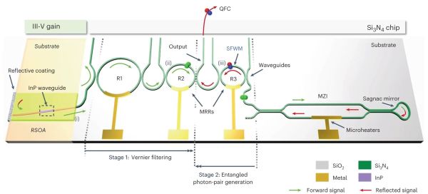
As the world of computing and communication draws ever closer to a quantum future, researchers are faced with many of the similar challenges encountered with classical computing and the associated semiconductor hurdles. For the use of entangled photon pairs, for example, it was already possible to perform the entanglement using miniaturized photonic structures, but these still required a bulky external laser source. In a recently demonstrated first, a team of researchers have created a fully on-chip integrated laser source with photonic circuitry that can perform all of these tasks without external modules.

In their paper published in Nature Photonics, Hatam Mahmudlu and colleagues cover the process in detail. Key to this achievement was finding a way to integrate the laser and photonics side into a single, hybric chip while overcoming the (refractive) mismatch between the InP optical amplifier and Si3N4 waveguide feedback circuit. The appeal of photon-based quantum entanglement should be obvious when one considers the relatively stable nature of these pairs and their compatibility with existing optical (fiber) infrastructure. What was missing previously was an economical and compact way to create these pairs outside of a laboratory setup. Assuming that the described approach can be scaled up for mass-production, it may just make quantum communications a realistic option outside of government organizations.

Neural Network In Glass Requires No Power, Recognizes Numbers

We’ve all come to terms with a neural network doing jobs such as handwriting recognition. The basics have been in place for years and the recent increase in computing power and parallel processing has made it a very practical technology. However, at the core level it is still a digital computer moving bits around just like any other program. That isn’t the case with a new neural network fielded by researchers from the University of Wisconsin, MIT, and Columbia. This panel of special glass requires no electrical power, and is able to recognize gray-scale handwritten numbers.

Continue reading “Neural Network In Glass Requires No Power, Recognizes Numbers”