Dirty little secret time: although amateur radio operators talk a good game about relishing the technical challenge of building their own radio equipment, what’s really behind all the DIY gear is the fact that the really good stuff is just too expensive to buy.
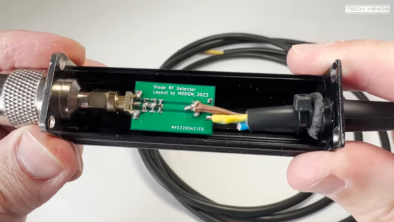
A case in point is this super-low-cost RF power sensor that [Tech Minds (M0DQW)] recently built. It’s based on a design by [DL5NEG] that uses a single Schottky diode and a handful of passive components. The design is simple, but as with all things RF, details count. Chief among these details is the physical layout of the PCB, which features a stripline of precise dimensions to keep the input impedance at the expected 50 ohms. Also important are the number and locations of the vias that stitch the ground planes together on the double-sided PCB.
While [Tech Minds]’ first pass at the sensor hewed closely to the original design and used a homebrew PCB, the sensor seemed like a great candidate for translating to a commercial PCB. This version proved to be just as effective as the original, with the voltage output lining up nicely with the original calibration curves generated by [DL5NEG]. The addition of a nice extruded aluminum case and an N-type RF input made for a very professional-looking tool, not to mention a useful one.
[Tech Minds] is lucky enough to live within view of QO-100, ham radio’s first geosynchronous satellite, so this sensor will be teamed up with an ADC and a Raspberry Pi to create a wattmeter with a graphical display for his 2.4-GHz satellite operations.


Scottish Diode :) at 6:33m
“Dirty little secret time: although amateur radio operators talk a good game about relishing the technical challenge of building their own radio equipment, what’s really behind all the DIY gear is the fact that the really good stuff is just too expensive to buy.”
The other little secret is that it takes expensive test equipment to be able to build DIY radio gear much beyond simple projects, like the example posted. This is especially the case when building something that transmits, since it is important not to pollute the airwaves with spurious RF emissions! As the transmit frequency goes up, so does the cost of the test equipment.
I discovered this from my own experience. YMMV. Apologies for sounding negative. I’m just being realistic.
Pretty much while I cover just DC, audio, and low frequency microcontrollers. Even as a ham I leave the higher frequencies to those devices built by professionals who have already invested in the necessary test equipment and facilities plus meeting regulatory requirements.
Really like the article, though saying
> Chief among these details is the physical layout of the PCB, which features a stripline of precise dimensions
is like, describing car design,
> Chief among these details is the physical design of the chassis, which features a set of wheels that need to be making contact with the ground
Not a detail – it’s the working principle of a stripline. In fact, the working principle of basically any transmission line, and their connectors. (That’s why the nice type-N connector is probably more expensive than the rest of the device – precise dimensions that don’t change under temperature variations, mechanical stress and moon phase.)
Sure, but PCBs aren’t as strong in the zeitgeist as cars are. Most people don’t even know what a PCB is (electronics simply go brrr to most), let alone that there need to be any design considerations for AC. While the average hackaday reader will know more about this than the average world citizen, AC and RF design are on the edges of many of our knowledge envelopes, and striplines, impedence matching, etc, are just a couple of many aspects of AC design. As such, mentioning how it works is extremely reasonable.
Absolutely agreeing with you! The framing of the working principle being a detail is what I considered a bit funny. (And I mean funny! :) )
To express what you’re saying a bit more pointedly: It’s important to mention the inner workings of things – and pinpoint the important core concepts that make things work. Because otherwise, a magical thinking of “anything that’s inside the black box is a detail, and all of them are equally unimportant”.
Compare this (which is easy for me, I’m an electrical engineer, and while I’m not the worst with cars, I honestly don’t care for them at all):
Imagine someone who’s not been told in school or family that a car has a motor, which burns fuel to move pistons to drive gears to drive an axle to move the car, but has been driving a car for a while. Now, someone opens a modern compact car’s motor compartment, and asks that person to pinpoint the most important part in there, how high are chances it’s going to be the visible parts – the battery connectors, the fusebox, the fan of the cooler, and not the actual motor that’s hidden beneath a black plastic cap with the car manufacturer’s logo on it?
So, knowing that a motor makes the car move is not a detail, if you want to understand the priciple *how a car runs*. Calling the presence of a motor a detail wouldn’t do that principle right.
At the same time, we’re calling a transline, which takes the signal, together with the lumped components matches it to a diode and acts as the filter on the output, a detail to someone who’s built an RF power meter. Eh.
How much power can it handle?
The video shows up to 16 dbm, but of course you can use an attenuator in series as well.
That also happens to be the range the original designer tested¹ it with. And I wouldn’t go far beyond that! Higher power means higher voltage, and higher voltage means near-exponentially decreasing capacitance for a diode².
Also, higher power means hotter diode. And all semiconductors are very good thermal sensors³. It’s just that with enough to respect that, you can also build other, sometimes more useful functions out of them ;-)
—————————————————————————————————————–
¹hesitant to say DL5NEG “calibrated” it, because calibration kind of comes with the expectation that you tell me which standard you’re comparing with, and while the video author is fine with the strongly held belief that their RF circuit is similar to what DL5NEG built, based on a reproduction of a hand-drawn scale drawing without explicitly marked dimension, reproduced on completely different board materials, I’m not. “Roughly 10 dB, and that’s also what I’m seeing”: great, you could have just as well guessed…
Now I believe that DL4NEG has something to measure against – either a calibrated power source or a calibrated power metering device – it’s just that the video annoys me in hard to reach places, as building a measurement device and having no better assessment than “I believe my SDR does roughly what I’m supposedly measuring is really not very trustworthy.
² 1SV305 type diode’s C vs V curve: https://i.stack.imgur.com/bR73D.png this has the potential to produce a serious mismatch at the input. NB: that graph’s vertical axis is *not* linear!
³ all semiconductors have charge carrier mobility (i.e., effectively conductivity, which does dominate their ability to rectify efficiently) that’s exponential to temperature. In RF applications, a change in temperature also effects a change in capacitance.
Quick correction since the author and the comments don’t seem to be getting it right- that is a microstrip line – stripline by definition is a TEM mode buried in the PCB itself with a ground top and bottom.
I do like this little hack. It’s nice. It would be a lot easier to put together using wire solder and two soldering irons, maybe a little board heater underneath would be nice too. For users at home I wouldn’t waste my time with a hot air gun for this application the parts simply aren’t complicated enough.
There were a couple comments about power handling above- The author mentioned he has a couple on his transmit line and will be using attenuators to set the input power to this meter. That’s how it works in test, measurement, and commercial installations, including cellular. Cool hack!
I really appreciate the beauty in just how cheap this design was put together. A handful of discreet parts and a really cheap PCB. This falls into the novelty level of using a $10 RTL SDR for spectrum analysis, and 6.5-bit ENOB aside, some spectrum analysis for 10 bucks is kind of amazing!
I would like to argue that I could do better with an LTC5518 or LT5534, and performance-wise I can, but it comes at a higher cost and will require calibration against that high price test equipment some other commenter mentioned. So there’s that.
Dust settles- very impressive for $10 or $20 hack. Some power meter is better than no power meter.
absolutely beautifully said!
Re: 20€ power meter that incorporates temperature compensation and an (optional) RMS circuit: build the reference circuit from the ca. 8€ analog devices ADL5904 ‘s datasheet ;)
https://www.analog.com/media/en/technical-documentation/data-sheets/ADL5904.pdf
0.5mm pitch says you really want that board to be manufactured, not self-made, but is pretty manageable.
(are the old linear parts still available? I was browsing for RF power detector ICs a while back and the cheapest ADI, which by then had already aquired LTC, had to offer was essentially the ADL5904, which I could easily imagine being a product line continuation.)
While I find the project interesting to reproduce, I agree with you that you shouldn’t trust it to perform the same way than the one from DL5NEG.
A way to reduce the effect of using different PCB materials/processes would be to use a coplanar waveguide type of transmission line. It would reduce the effect of the substrate dielectric constant because the wave is partly propagating in free space. But then you would have to remove the soldermask and start to worry about which surface finish to use.
About the temperature, I’ve seen another take on the subject from the
All Electronics Channel on youtube, he is using a dual schottky BAT15 in a single package. One is used for the detector, and the other is used as a temperature sensor. He then uses a resistor to heat and regulate the temperature of the sensor.
https://www.youtube.com/watch?v=sAa1uHSF7Ew
True, lower dependency on the substrate.
But that would require you to a) achieve some ~ 0.1 to 0.2 mm gap on a board and b) remove the ground plane below the line, otherwise it’ll be a coplanar waveguide with ground, which would still be pretty dominated by the ground and thus the substrate.
So, that would, in exchange for reducing the depenency on the board material, increase the dependency on exactly reproducible manufacturing. Not trivial at the least end of board pricing!
(I can’t reply directly to you latest reply Marcus, probably too much nested replies).
I don’t think it would increase the requirement on manufacturing accuracy. No matter the dielectric, the geometry has the same effect on the final impedance. Or I am missing something (which is quite possible)? The requirement maybe more more about the layer engraving accuracy for CPW than the dielectric thickness but both are needed in both cases.
Anyway PCB services nowadays can perform quite well for very cheap. PCBway and JLCPCB offer around 0.1mm minimum spacing for cheap. The actual spacing is probably not really precise nor repeatable, but it could be tested by ordering different batches from different PCB services.
The question is how close would a reproduced device be from the one on the internet without performing another calibration, and I think you can achieve some accuracy that would be acceptable for hobbyist grade equipment. Besides the transmission line impedance control, there is also the issue of variability in the diode characteristics and the passives.
Maybe we could perform some kind of calibration fine tuning by testing the device with “cheap” lab equipment (curve tracing the diode, measuring the gain at DC or low frequency, …) to transfer one properly made calibration on a reference design to a reproduced device. ML algorithms could help with that.
Anyway, any article that causes me to think about such things is a good article in my book. And it’s refreshing to see this when compared to a couple of awfully bad articles that I saw in here recently.
PROTIP: before printing PCBs for etching check if your laser printer preserves dimmensions accurately enough. Mine is fine in vertical but horizontal dimmensions needs to be multiplied by 1.012
I think the original board was scalpel-cut of a plain copper-clad board, but: Good tip!
But I honestly think we’re collectively in the process of leaving the toner transfer or transparency exposure methods behind for most use cases. Even domestically produced PCBs are just cheaper than the chemicals involved and the mess, and the equipment needed, unless you’re doing a lot of boards per year, in which case you’d be cursing a lot if you’re doing them yourself. (Of course you can perfect your technique, have a great bubbler, just the right printer, the right toner, the right transfer material, the correct timings, the perfect handling and cleanup procedure… but then you’re around a 1000€ into your hobby, for which you could have ordered 50 to 300 different boards that are qualitatively still superior, and have stop mask, drills, come with a solder-ready finish.)
Sure, there’s a lot of beauty in “build your own darn birdhouse”, just that this particular kind of birdhouse is pretty fiddly to build well, even if you built it well, the cheapest custom commercial birdhouse is cheaper in practice, and waaaaaaay better, and the birdhouse has the tendency to leave permanent Iron-II stains and produces toxic heavy metal sludge. I don’t know whether there’s not other birdhouses I’d prefer to build…
I think we all want to see what the connector is at the other end of the mains flex …..
The video shows stripped wires. He attaches spring clips (mounted on his DVM test leads).
That gave me a momentary panic attack, seeing an RF connector at one end, all but directly connected to a mains cord.
Use solder paste, leaves a pro finnish and it’s quick and easy, those joints look rough
I did something similar with a microwave diode HSMS-2850, works well as long as you have friends with precision equipment where you can calibrate it. The schematics here has one shortcoming though it’s DC coupled that means that any DC bias will make it to the diode and produce completely wrong results. Mine is AC coupled with two 47p capacitors in series right after the connector to cut off any DC voltage.
solder
Where can I find that wonderful case? My projects involving N-connectors always look a mess.
Man, I hate to say it, but this is an an example of a good foray in into RF design that is absolutely killed by that terrible solder job. Most of the gains he could have had by the semi-professional PCB is likely ruined or at least greatly diminished by the solder job. I deal with similar stuff for work and poor vs good solder absolutely can change a 1dB loss into a 10+dB even using the same pads. Honestly, that it ended up that bad even on a real board makes me slightly speechless…