When it comes to things that hackers build, PCBs are a sizeable portion of our creative output. It’s no wonder – PCB design is a powerful way to participate in the hardware world, making your ideas all that more tangible with help of a friendly PCB fab. It’s often even more lovely when the PCB has been designed for you, and all you have to do is press “send” – bonus points if you can make a few changes for your own liking!
A lot of the time, our projects are untrodden ground, however, and a new design needs to be born. We pick out connectors, work through mechanical dimensions, figure out a schematic and check it with others, get the layout done, and look at it a few more times before sending it out for production. For a basic PCB, that is enough – but of course, it’s no fun to stop at ‘basic’, when there’s so many things you can do at hardly any cost.
Let’s step back a bit – you’ve just designed a board, and it’s great! It has all the chips and the connectors you could need, and theoretically, it’s even supposed to work first try. Now, let’s be fair, there’s an undeniable tendency – the more PCBs you design, the better each next one turns out, and you learn to spend less time on each board too. As someone with over two hundred PCBs under her belt, I’d like to show you a bunch of shortcuts that make your PCB more helpful, to yourself and others.
There’s a few ways that you can share your PCB projects in a more powerful way – I’d like to point out a few low-hanging fruits, whether README.md files or markings on the PCB itself. I’ve been experimenting quite a bit with external and embedded documentation of PCBs, as well as PCB sharing methods, got some fun results, and I’d like to share my toolkit through a few punchy examples and simple tricks. I’d also like to hear about yours – let’s chat!
Furnish It
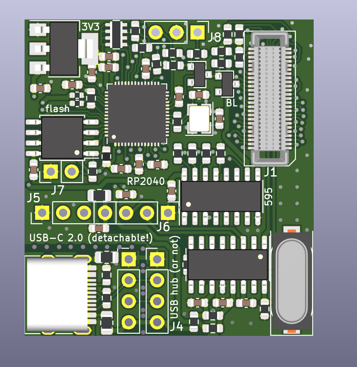
 Most of us start with a PCB covered with reference designators, and that’s fine – it’s the default for many PCB tools, after all. Make sure you’re not forgetting a few important things, though! After all, blank PCBs are indeed mysterious, but it’s a bit of an artform to pull off a blank PCB and not have it be a pain afterwards.
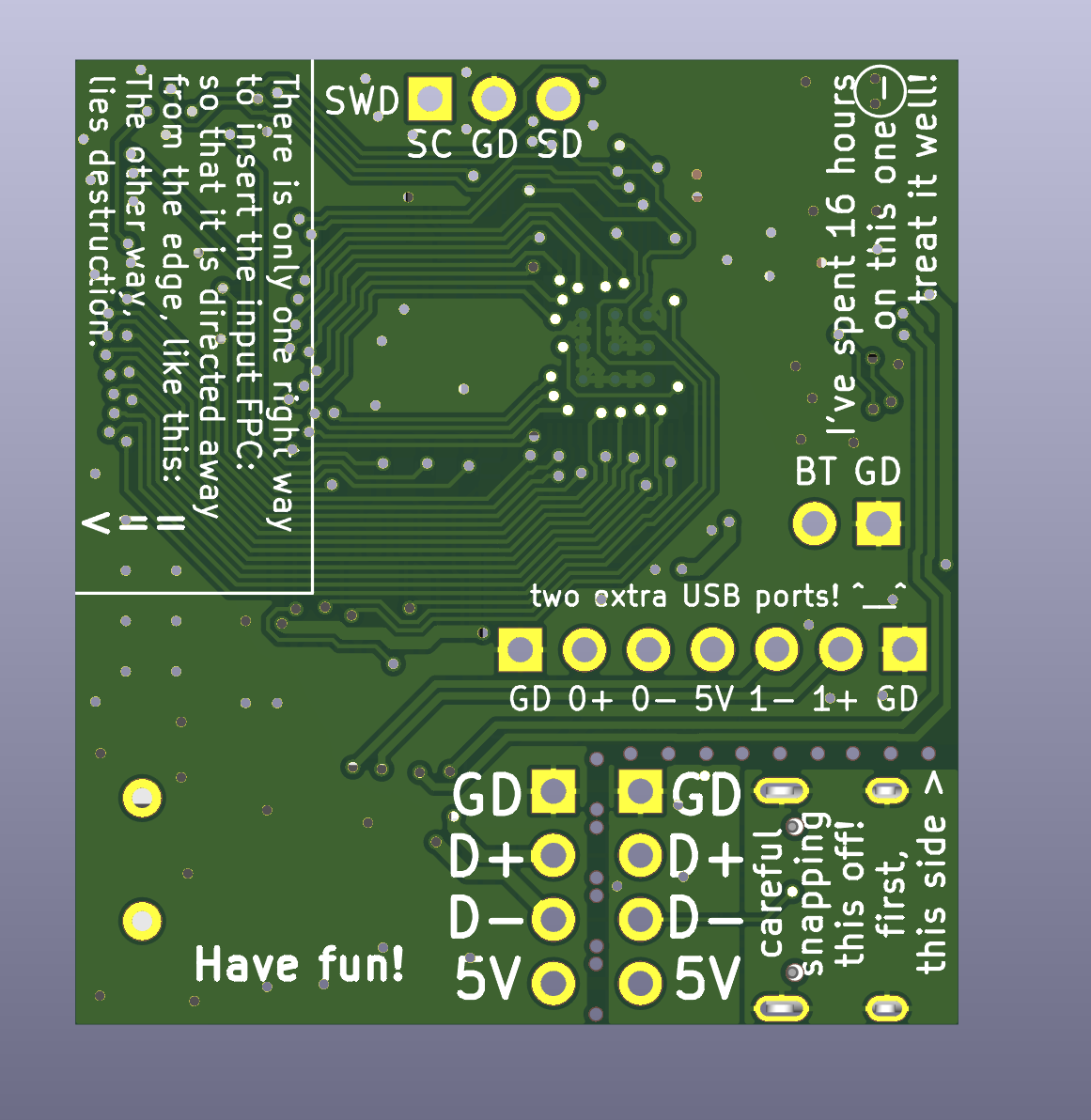
For a start, there’s a lot of place on your PCB, for things you might not have thought of. You will forget some things, you will mix some things up, and any other person who you give it to, will know even less – if you use silkscreen in certain ways, you can make your PCB not just connect things together electrically, but also keep you informed about its purpose, capabilities and limitations.
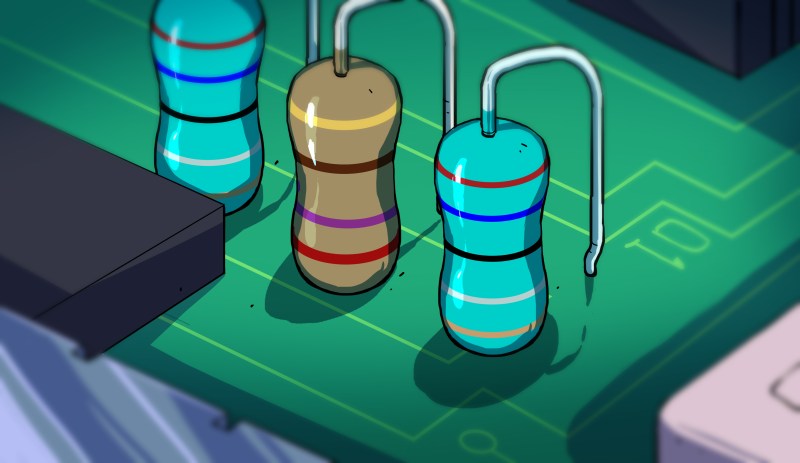
Is there a warning that users of your PCB should keep in mind, even if the only user would be you, but in the future? Put it on the silkscreen! For instance, input voltages and polarity for power connectors – if it’s not using some standard connector, be it USB or PS/2, at least putting small ‘+’ and ‘-‘ on the PCB is wonderful, and doubly so if you have a battery holder! Even if your input is USB-A or MicroUSB, which is a great proxy for “5V input”, it might be worthwhile to mark your amperage if your board would use more than 500mA-1A – since, often, USB ports can only provide that much.
Pinouts are useful to have as a reference, but they’re a kind of warning, too – an extra check before you plug something in. They also save a ton of time when you’re wiring things up – having to distract yourself and check a datasheet, a PCB image or even a KiCad window while soldering can sure slow you down.
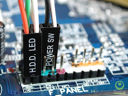
As a guideline, every connector deserves its pinout marked on the silkscreen, on all sides it could be approached from. Let’s be fair, if desktop motherboards would put pinouts for the front panel headers on the silkscreen instead of burying them in the manual, we’d all be just a tiny bit happier. In those moments when you have the PCB on your hands and you’re eager to put it to use, it’s a bit frustrating to have to refer to the user manual for pinouts – and so often, there’s a way to fit them on the silkscreen, putting in a bit of care for the future you, or anyone else you’ve entrusted with a PCB of yours.
Of course, you might not always have space. That said, you can still do abbreviations – the QWIIC-like “GND VCC SDA SCL” can be shortened to “G V D C” if you must. You can also do things like changing pad shapes to delineate different power pin types – for instance, always use the square pad for GND. Oh, and the silkscreen isn’t the exclusive place for your text – you can put on text on the soldermask layer for either silver (HASL) or golden (ENIG) lettering, or perhaps, do higher-resolution text on the copper layer if you have enough PCB space. You can even put markings on the copper inside your pads, remember?
Do you need to add all of these? No! Do you want to add at least some of these? Absolutely! Pick the things you feel like are easy for you, make them into habits, and you’ll quickly gain skills in making your boards speak for themselves.
Dereference It
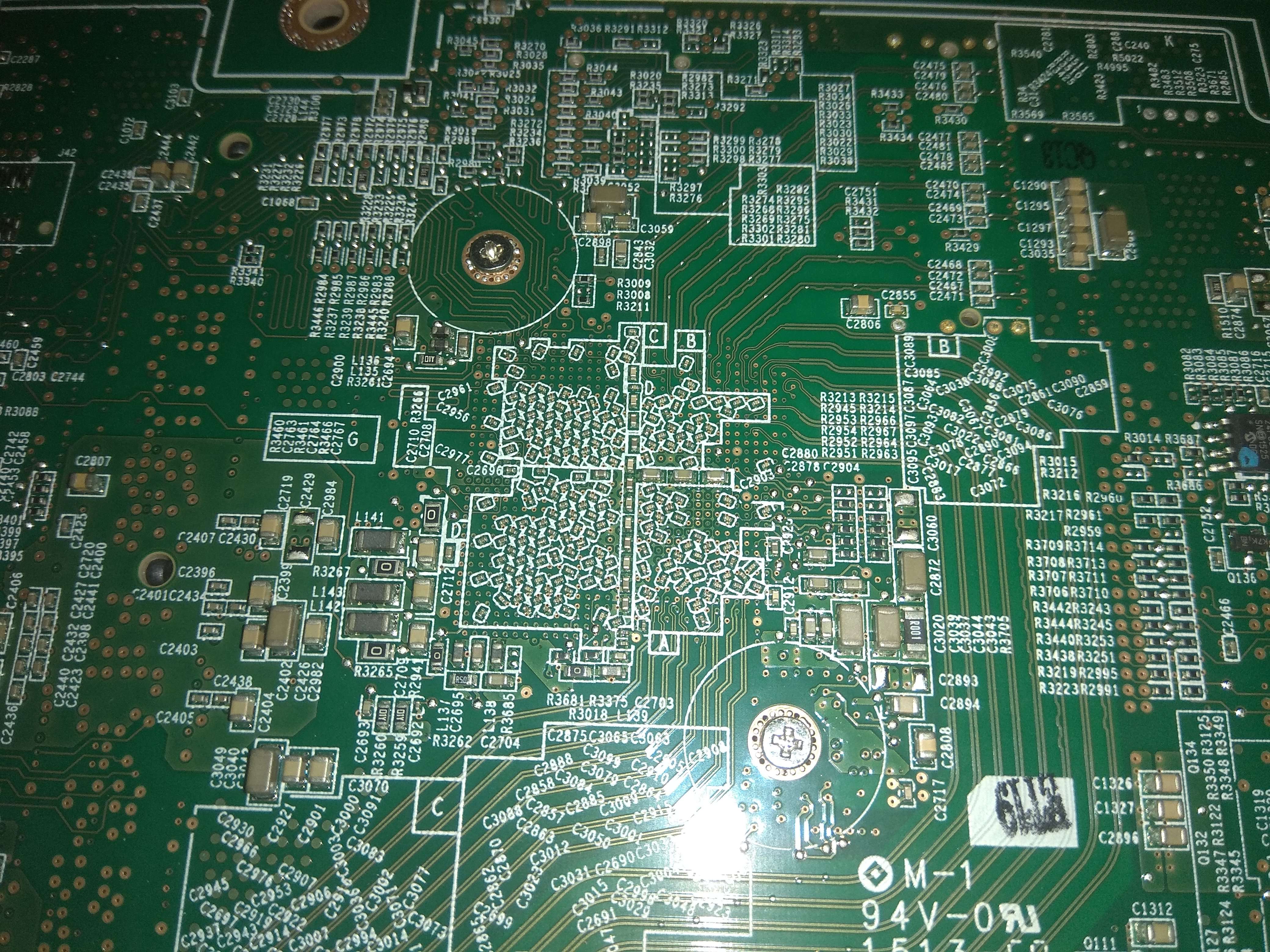
Here, I’d like to argue against putting reference designators on your PCB silkscreen- you know, things like R3 or C149. Unless you have heaps of space on a board, consider this – there’s lots of other things that take priority, and the more packed your board is, the smaller is the amount of place you have for these things.
Reference designators contain a ton of information, they’re visual clutter, arranging them takes a good chunk of time, and they’re exceptionally situational. From my experience, pinouts, instructions, warnings and descriptions are worth their weight in gold, and reference designators just, aren’t. Sure, the user might be interested in knowing that the barrel jack is marked J1 on the schematic, but do they know what voltage range is it intended for? Which one would you like them to keep in mind? Which one of these would you want to quickly check as you experiment?
 Erasing all reference designators is super straightforward. Afterwards, you’re left with a ton of extra space – somewhere you can put your pinouts, instructions, diagrams, or even hopes and dreams. I personally don’t put reference designators on boards, and if you haven’t yet considered removing them, I recommend that you do.
You might argue there are good reasons for reference designators sometimes, and to that, I agree – it’s just that they’re situational. Your board house shouldn’t need designators – a large amount of PCBs are nowadays released without them, anyway, and you can always provide them with a PCB picture that has the F.Fab and B.Fab layers exported instead. Thinking about releasing rework instructions for your userbase? You should provide pictures either way.
I usually leave reference designators for things like jumpers, crucial parts like user-adjustable current setting resistors, and connectors – beyond that, it makes little to no sense to have references taking up space on the silkscreen.
Describe It
Now, there’s something that’s often missing from published PCBs – and that is a README file. It’s a bit painful to open a Github link and see nothing but a <code>kicad_pcb</code> and <code>kicad_sch</code> file – these are sufficient, but I’d like to know more about what your board does, beyond the filename. and it’s not hard to add either!
Let’s say you’ve just designed a PCB. You’ve just put a metaphorical point in your project, and you have the entire context in your mind still, and it’s a satisfying point to be at – ain’t that wonderful! While you have ever aspect of the board available on a moment’s notice, open a README file in your text editor and spend a minute-two dumping your brain’s contents into a text file. What does your PCB help with? Which chips or parts are crucial for its purpose? Isn’t it wonderful that the PCB is done, and don’t you want the world to know about all the cool features you added?
So, write it all out, as much as you feel like it, but write something. You only really need a sentence or two for a sufficient README, and if you’re not too tired, you might find yourself writing a few more. However many sentences you write, it matters that a README is there. I personally start with a template that lists a few commonplace board things and pre-filled metadata fields, and also has things like disclaimers about the design being untested or unfinished – quite worthwhile to have!
There’s more uses for a README – for instance, whenever you’re releasing a new version, you can add a section describing what changed, what got fixed, what got added or removed – just put them as bullet points in the same README. This helps in debugging, and also informs the user that there’s more than one version of this board in existence.
Name It
Some of my personal projects are on their fifth revision, with the PCB’s looks having long stabilized. Having the version number on a visible spot has been a lifesaver of a practice – especially when I’m dealing with a PCB where v2 just works, but v1 requires an intense magnet wire fix. Unlike with software, the PCB version can be a single number – the PCB release cycle is way slower than software, so things like semver would just be wasted PCB space.
With my PCBs used by me a lot, and sometimes even used by other people, I’ve come to a short naming formula that works well. On the silkscreen, I put “BOARDNAME by AUTHOR, vVERSION” – for instance, “PS/2 to USB adapter by Arya, v1”. It’s short and sweet, and even if you don’t have any energy to work on the board’s silkscreen, perhaps this is the thing that can stay.
With PCBs, sometimes you want to share them with everyone else, but even if you don’t intend to, you still have to share them with you from the future. These few aspects matter, and as you learn to prepare , you’ll find that your work is more useful to others than ever.


If you don’t want to delete all refdes markings, just delete decoupling cap refdes markings and replace them with a single letter/symbol that designates what they are, and document that somewhere on the board.
Decoupling cap refdes markings are pretty much the least useful of any since so many of them are identical. Labelling them differently also helps visually because if someone says “oh, a component’s missing, but it doesn’t have a refdes” you immediately know it’s just a decoupling cap (which obviously *could* cause problems, but is less likely than almost any other component on the board).
Using refdes groupings (e.g. RA1, RB7, etc.) instead of straight incremental (R1, R743, etc.) also dramatically increases the usefulness of refdes markings.
One thing I’ve found useful (and takes up very little space) is a compass. Then it’s easy to refer to the North/South/East/West side of the board (and components thereon).
That’s a GREAT one!
I can see why a board in production might not need reference designators but I’ve certainly found them helpful when a) hand stuffing a board and b) debugging a board. It saves the step of having to reference another document.
This is also a good argument for common designators for decoupling caps and reference designator groupings, too. It’s easy just to scan the board looking for “A” and place all the decoupling caps at once, and easy to find a refdes in a schematic if it’s logically grouped rather than incremental.
It’s especially helpful when troubleshooting a board with another person who is looking at schematics. It’s a lot easier to say “what’s the voltage across R23” than having to point out passive components that look like ants in an ant farm.
Good recommendation to identify components on the PCB. However, just don’t use the goofy cryptic coding used on the resistors in the article’s picture.
I’ve got to disagree. If you want other people to use your PCB layout, leave the part designators on it.
You are drifting far into appearance over function when you remove the part designators to “make it less cluttered.”
The PCB is only looked at when assembling or debugging – in both cases, the part designators are a help.
Take a few minutes to tidy up the board by putting the designators in reasonable places instead of just deleting them and making your own life more difficult.
Strong agree.
I don’t design many boards at work or as a hobby but I do assemble plenty (for both) and removing the part designators is a terrible idea. You might easily remember where everything goes, but I’m not a mind reader and it’s way quicker if they’re there.
I’ve been creating, assembling and troubleshooting PC boards for a VERY long time, including some extremely dense layouts produced in the millions, and I find reference designators essential on all but the most rudimentary designs. Once I read a recommendation that they should be deleted, I had to ignore the remainder of the article. I don’t understand what experience would lead to this conclusion.
Some good tips in the article, but I would agree that reference designators are an absolute minimum standard of documentation wherever possible. (For some layouts it’s not.) Pictures or graphical layout aids are not a substitute; anyone debugging, servicing, or modifying the board should be able to quickly correlate physical circuit elements with the schematic and BOM.
Take a look at the backside of a major current-draw device, like the CPU in a game console/laptop or an FPGA. There are decoupling caps on every single power via, because that’s what’s recommended. They are all the same. There’s nothing special or unique about any one of them. They’re completely interchangeable, and the only reason there are so many of them is, well, inductance sucks.
There is absolutely zero need for any of those caps to have a unique identifier. None. They’re completely identical on the schematic.
I made a board once (Logic Noise Klangorium up on IO) that had all the same resistor values except for two or three. I took off the value designators from all of the common ones.
Problem is, you then have to be explicit in the directions and say “all values that aren’t marked are 100k”, and the people assembling the board have to read that and remember the value. So it’s really just shifting the documentation off the board and onto the webpage. And I think, in retrospect, that’s the wrong place.
I can imagine the same happening with the decoupling caps. What value should I use for them all? 0.01 or 0.1? You’ll have to specify that somewhere, and I have to go look it up.
I’m totally down with values “100R” instead of reference designators “C442” though. That puts the information in one place, and it’s the place that it’s needed.
“What value should I use for them all? 0.01 or 0.1? You’ll have to specify that somewhere, and I have to go look it up.”
You use single letters or symbols, one for each cap type (skipping the standard confusable letters obviously). So “A” caps are 0.1 uF 0402 3.3V rail. Then you put that legend in an open space on the board. Generally if you specify the rail you don’t need to specify the voltage rating of the cap.
Resistors are different than decoupling caps, though. They’re not unique. There might be a time when you want someone to check a value on a specific resistor, like “if it’s not working, check the voltage across R23” and it needs to be *that* resistor.
Decoupling caps are identical from a debugging standpoint. The only time you ask anyone to check across it, you don’t care which one they do it across.
That’s fine unless you find out later that you have to change the resistor value. Maybe further testing showed that you needed a stronger pullup, or a voltage divider needs tweaking. Much easier to just update your docs than order a new PCB revision.
KiCad has some awesome plugins for assembly help when you’ve removed your refdes’. I’m 100% on board with that suggestion! InteractiveHTMLBoM is my plugin of choice for this work. Otherwise I plant the reference designators on the f.fab layer and print it out on a sheet of paper. Components can then be visually referenced. This has been the fastest way, I’ve found, to prototype 10+ component PCBs.
If your project have VCO or any oscilator soldered on PCB, avoid it’s heating and cooling together with other parts on PCB however you know if stable frequency is important. Made some holes around, conect gnd around and below it with thin connection to other parts of PCB.
Even big manufacturers made error and place it close to other component that change temp.
We version our boards and then add a moderate sized big white box in silk for people to write in. On my own boards I add a little serial/i2c eeprom and header and put incremental modification notes in there. And my usual mention of soldermask cutouts and metal layer numbers on each layer so when you hold it up to the light you can see if the stackup is what you asked for or if they mistakenly put all ground on one layer and that’s why nothing works. This is pretty unlikely but I’ve encountered it twice. (“But we ran it through our board checker” yeah your board checker only checks for opens not node to node shorts apparently)
I have coworker who put the refdes under the part on really packed boards. I’m definitely in favor of rooms or by-page numbering, so all the stuff associated with site 1 have a R1xx/C1xx and site 2 is R2xx… Much easier to debug, and many schematic programs support auto annotation that works this way.
I love the EEPROM idea! Obviously not for all designs, but the “revision notes built into the PCB” is a good idea. For certain microcontrellers you could probably also put a txt file on there…
I’d suggest that the square pad on a connector doesn’t designate ground, but merely indicates “pin 1”.
I would certainly agree with that! It’s been done for decades. Anything else would be a backwards step. However, I would be in favour of an octagon, or hexagon, or round with one flat side… what is that shape? I’m sure it has a name…
Oh, and speaking of pin 1… for several years now I’ve been putting a small triangle (on the copper) next to pin 1 of connectors where there is no opportunity to mess with the pad shape. FFC/FPC connectors are a prime example. No markings on the cable OR the connector makes debugging very hard: now which end is pin 1?
Me too! I usually put an arrowhead or a dot next to pin 1 on the silkscreen.
I put a little circle on the silkscreen – nothing conductive to get in the way. Kicad 7 will also let you “group” parts so that you can move the footprint and your little circle simultaneously if you have to move the IC as your design evolves.
I also REALLY try to have pin1 of ICs in the same orientation on the PCB, e.g upper left (or North West, if you’re using the excellent “compass” suggestion above)
Nice article.
I was thinking for my last PCB of including a QR code that provided some self documentation. Looks like a (big) QR code can hold 3kB of data, so probably not enough to hold a schematic file directly, but maybe with some compression tricks you could include a compressed .png of the schematic or something? Would probably be enough for the “readme” file brain dump mentioned in the article.
Of course the QR code could link to the documents, but then you have to commit to having them in the same place forever.
Love the idea in the comments of an onboard serial EEPROM though!
Think of it as a challenge worthy of demos of old. 3kb for a schematic.
Why not use IPFS? Could use the Cloudflare gateway!
Half my reply:
My advice for component designators (R3, C6…) would be not to include them, but in their place do put, in the very smallest silkscreen text your fab can print (they often claim 1mm letter height, but I find 0.7mm prints ok for vector fonts with thickened line widths), the value next to each component. This really eases hand assembly, you can look straight at the board to see what must go where. For IC chips put the part number under it, no need for a U1, just say it is a 555, this helps guide you during assembly more easily than glancing aside at a diagram on screen, or even worse, at a spreadsheet listing what value C7 is to take. In any section of the board keep all value markings in the same relative orientation to the part they relate to, so you don’t have the value to the left of one thing and the right of the other. For passives, have the text running parallel to the longest axis of the part. For polarised parts always ensure polarity markings are clear and obvious, and try and have all polar parts on the whole board aligned in the same direction. And where you have say only one type of sot-23 transistor on the whole board put a note in free space saying what model of transistor is used, and just leave each footprint unlabelled. Or if you have a load of one sort of diode, put one comment in silkscreen saying what type it is, and at each instance just indicate polarity with the diode symbol. I’ve done this on very dense PCBs, ones with very tight mechanical constraints to the extent both sides were covered in 0603 and tssop parts, and still found room for value labels to be just about readable.
I’m a software guy first, but play an ee not on YouTube or tv. To me, the silkscreen has been like commenting code. RobertP’s comments most align with where I’ve been heading with my pcb designs. However, the idea of fitting the schematic into a QR code takes the self documenting idea to the next level! I think decoding it would be a pain though, so probably not worth it. Though it may be fun to play!
Either way, I think this comment thread has some of the most useful ideas I’ve ever read. I avoid comment sections on most posts and most websites, but I’m not disappointed at coming to this one.
Was the suggestion to remove the ref markers an example of Cunningham’s law? If so, it worked marvelously. Not only did people bite on that point, but then went on to offer so many more suggestions. Bravo!
Second half of my comment:
Values being shown are useful for aiding assembly, whereas part reference numbers are a bother and don’t actually help in debugging. That is to say, if you are trying to trace a trace around a board and compare it to the schematic you should have labelled diagrams of the schematic and board layout to hand on screen, these will make it apparent where the 15K ohm resistor sits just as well a R8 would. And in the case of reverse engineering PCBs without documentation present, well then the designators are totally useless as you have to build the schematic yourself from tracing anyway and knowing the numbers the original designer used will tell you far lessthan quickly seeing the values. One extra tip, your values don’t usually need to declare if the part is a res or a cap, it will be obvious from the size of the number, 1u or 22p are obvious caps, 3K3 and 560K are obviously resistors. For resistors under 1K I usually use “R” in place of K or M. Maybe a 10u inductor might need an L or a H in the marking, L10u or 10uH maybe, to avoid confusing with a 10u cap, but you probably only have one or two inductors on a board, if any, and they’ll likely be a very different form factor anyway. The only downside I can note is that this works fine only so long as you don’t have a board where you have for example a mixture of two different types of 1uF 0603 caps but which have different voltage ratings or accuracy tolerances, but in low volume hobbyist and prototyping and academic uses you probably aren’t trying to mix and match parts of the same value and size just to marginally reduce costs by speccing each part only for exactly what it needs to cope with and using cheaper lower rated passive parts in specific places on the board.
I’d put the values of the no-brainer components, and names for ones with more thought behind (an inductor with special saturation behaviour, a timing resistor matched to that inductor, variants with different components on the same footprint, …). That said, the one time I could have used that scheme the board was 2-layer-and-solder-stop-only, so I had only a name, title and version on a ground plane…
While every youtube influencer includes at least one ad for an overseas PCB manufacturer, remember the tradeoffs when sending your designs to them. It’s cheap for a reason. Furnish, dereference, describe, name … all good practice when you have a trustworthy partnership. Otherwise, remember the most important one: Obfuscate-it. Even consider physically breaking a board up and send each module to different manufacturers. Be warned they may all be the same manufacturer however. If you don’t mind a copy of your design going up on taobao, 10 boards for $5 is a steal.
Depends on what you’re making. At some point, I’m going to make a voltage controlled current source for RGB lasers that will fit in the footprint of the crappy rgb laser driver I got that PWM’d for color…not great for use with a galvo scanner! I’d very much like for them to copy and paste that thing onto every rgb laser they sell. That way, the next guy who gets it in his head to start a project with such a laser, actually finishes it and we all get cool stuff for it. (Of course, I also want to be able to take feedback sensors and some other safety items…and still fit in the footprint! One of these days…
I never put reference designators on my PCB’s. Not having them gives the PCB a clean look. I also use assembly drawings which show the part value and designator. When a BGA is used and there are 0201 or 0402 packages under the BGA (opposite side of board) it is nearly impossible to put ref des that makes sense. I do like other info on board such as connector pin function. Jumper setting info etc.
Who cares about a “clean look” on a PCB that is hidden inside something?
Put part designators on the board.
“Clean design” from back in the day.
https://youtu.be/YYqTCLMN_KI
I guess the article referres to the case when your board is so densly packed, that there is literaly no space to put your silkscreen on. If you have five different designators in the same space that is not helpfull anyway.
If you have tones of space you might as well put them on there.
Another thought: Nice, working, robust Technology allways looks nice in my opinion. (Of course, allways in its own way). So if it doesn’t look nice ….
Fight me! ^^
Yeah, that’s a fair argument but that’s not what the article is advocating for, quite the opposite. The author says to remove them *unless* you have bags of space left and want to put them on.
Just a thought, as with code, be mindful of the people downstream of you that might have to maintain or amend what you’ve created. A comment or a label never killed anyone but it sure might save a lot of headscratching later.