Share Your Projects: Making Helpful PCBs

When it comes to things that hackers build, PCBs are a sizeable portion of our creative output. It’s no wonder – PCB design is a powerful way to participate in the hardware world, making your ideas all that more tangible with help of a friendly PCB fab. It’s often even more lovely when the PCB has been designed for you, and all you have to do is press “send” – bonus points if you can make a few changes for your own liking!

A lot of the time, our projects are untrodden ground, however, and a new design needs to be born. We pick out connectors, work through mechanical dimensions, figure out a schematic and check it with others, get the layout done, and look at it a few more times before sending it out for production. For a basic PCB, that is enough – but of course, it’s no fun to stop at ‘basic’, when there’s so many things you can do at hardly any cost.

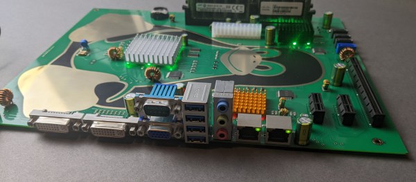
Let’s step back a bit – you’ve just designed a board, and it’s great! It has all the chips and the connectors you could need, and theoretically, it’s even supposed to work first try. Now, let’s be fair, there’s an undeniable tendency – the more PCBs you design, the better each next one turns out, and you learn to spend less time on each board too. As someone with over two hundred PCBs under her belt, I’d like to show you a bunch of shortcuts that make your PCB more helpful, to yourself and others.

There’s a few ways that you can share your PCB projects in a more powerful way – I’d like to point out a few low-hanging fruits, whether README.md files or markings on the PCB itself. I’ve been experimenting quite a bit with external and embedded documentation of PCBs, as well as PCB sharing methods, got some fun results, and I’d like to share my toolkit through a few punchy examples and simple tricks. I’d also like to hear about yours – let’s chat! Continue reading “Share Your Projects: Making Helpful PCBs”

An ATX motherboard sits on a grey surface with the I/O in the foreground. Behind the I/O is a large image of Tux, the Linux penguin, taking up most of the PCB and winding its way around different components on the board. Tux is part of the PCB itself, with his feet, beak, and outline in gold, body in black silkscreen, and belly in green soldermask.

Designing Aesthetically-Pleasing PCBs

We’ve seen our share of custom PCBs here on Hackaday, but they aren’t always pretty. If you want to bring your PCB aesthetics up a notch, [Ian Dunn] has put together a guide for those wanting to get into PCB art.

There are plenty of tutorials about making a functional PCB, but finding information about PCB art can be more difficult. [Ian] walks us through the different materials available from PCB fabs and how the different layer features can affect the final aesthetic of a piece. For instance, while black and white solder mask are opaque, other colors are often translucent and affected by copper under the surface.

PCB design software can throw errors when adding decorative traces or components to a board that aren’t connected to any of the functional circuitry, so [Ian] discusses some of the tricks to avoid tripping up here. For that final artistic flair, component selection can make all the difference. The guide has recommendations on some of the most aesthetically pleasing types of components including how chips made in the USSR apparently have a little bit of extra panache.

If you want to see some more on PCB art, check out this work on full-color PCBs and learn the way of the PCB artist.

Shot of CubeTouch, a six sided cube built out of PCBs with each of the top PCB allowing for diffusion of the LEDs on the inside to shine through

Keyboard Shortcuts At The Touch Of A Planetary Cube

[Noteolvides] creates the CubeTouch, a cube made of six PCBs soldered together that creates a functional and interactive piece of art through its inlaid LEDs and capacitive touch sensors.

The device itself is connected through a USB-C connector that powers the device and allows it to send custom keyboard shortcuts, depending on which face is touched.

Finger touching the top of a CubeTouch device

The CubeTouch is illuminated on the inside with six WS2812 LEDs that take advantage of the diffusion properties of the underlying FR4 material to shine through the PCBs. The central microprocessor is a CH552 that has native USB support and is Arduino compatible. Each “planet” on the the five outward facing sides acts as a capacitive touch sensor that can be programmed to produce a custom key combination.

Assembling the device involves soldering the connections at two joints for each edge connecting the faces.

We’re no strangers to building enclosures from FR4, nor are we strangers to merging art and functionality. The CubeTouch offers a further exploration of these ideas in a sweet package.

The CubeTouch is Open Source Hardware Certified with all documentation, source code and other relevant digital artifacts available under a libre/free license.

Continue reading “Keyboard Shortcuts At The Touch Of A Planetary Cube”

Dreaming Of A Transparent (PCB) Christmas

[Carl] wanted to put his force sensors on a transparent PCB and had to ask his board vendor for a special sample. Flexible PCBs are available on transparent substrates made of PET, but they are not as common as polyimide boards. As [Carl] found out, these boards are a bit thicker, a bit less flexible, and don’t hold up to very high heat as well as the standard boards. Undeterred, he designed a 3D Christmas tree using the clear boards. The result that you can see in the video below looks pretty good and would have been hard to duplicate with conventional means.

When you build the board it is as a flat spiral, but lifting it in the center allows it to expand into a conical tree shape. The circuit itself is just an LED blinker, but the flexible board is the interesting part.

Continue reading “Dreaming Of A Transparent (PCB) Christmas”

This CT Scan Of A PCB Is The Accidental ASMR We Didn’t Know We Needed

At risk of getting any ASMR buffs who might be reading cranky because there’s no audio, [Chris], or [@no1089] on Twitter, has gifted us with this visually stunning scan of his Maxim MAX86160 in-ear heart monitor mounted on a rigidflex PCB. You can take a look, in the video below the break.

If you’re wondering why anyone would scan a board, other than boredom, know that it’s actually quite common. X-Ray machines are commonly used as a quick, passive way to check a board that’s fresh off the production line. These aren’t the X-Rays like those of broken bones you’re (hopefully not too) used to seeing though, they’re Computed Tomography scans (CT scans, CAT scans), in effect just 3D X-Rays.

CT Scan of a BGA

For electronics manufacturers and assemblers, CT scans are incredibly useful because they provide a non-destructive way to check for errors. For example, how do you know if that middle BGA pin is actually soldered correctly? You could run a functional test and make sure everything is working (at least, everything you check), but that takes time. The longer it takes to validate, the higher the manufacturing cost. In manager speak: “cost bad. Fast good.”

It’s also common to use a CT scan to create a full 3D model of a board. This makes it easy to check every little detail, especially the ones that are visually obscured by surface mount devices or critical signal paths that are buried under board layers.

Highlight of solder joints on small-outline integrated circuit (SOIC) to a PCB’s pads.

If you want to geek out on CT scans, you can learn more about the lab that did this scan or by wading into this unclassified research paper from Australia’s Cyber and Electronic Warfare Division.

But we know you really want more of this video, but better. And we’ve got the goods. For the chill folk among you, here’s a 55-minute version without all the CT scan info cluttering the screen. For those of you currently blasting eDM in your headphones, here’s a 30 second clip of it looping at ~5x speed. Eat your heart out:

Continue reading “This CT Scan Of A PCB Is The Accidental ASMR We Didn’t Know We Needed”

Hack My Wired Heart

Liner notes? Passé. In Berlin, the release of a special edition synth-wave record came with an accompanying experimental synthesizer called Wired Heart.

At the core of this adorable heart-shaped synth, designed by music technology enthusiast [tobi tubbutec], is the classic 74HCT14 chip with six Schmitt trigger oscillators. The bright red PCB has eight gold touch and humidity sensing pads that activate and modulate these oscillators. As well as changing the sounds by playing with pressure and conductive liquids you can use the six sets of header pins on board to plug in your own components for noisy experimentation. Wired Heart ships with LEDs, photoresistors and a potentiometer, but we’ve also plugged our own DIY fabric pressure sensors into this synth to make some excellent electronic sounds.

In the Hackaday.io post linked above, [tobi tubbutec] walks us through a number of the circuit design decisions he made while prototyping his “cardiotronic human-touch hexoscillatric stereo esoteric snythespacer”. We enjoyed his creative and sometimes unconventional designs, from his inclusion of non-functioning traces for aesthetic reasons to his chosen method of hard syncing — injecting a small pulse of one oscillator into the other. If you want to examine his layout in more detail, [tobi tubbutec] has helpfully included the KiCad schematic file in his write up.

This adorable, hackable synth caught our eye at this year’s SuperBooth — an annual indie electronic music conference in Berlin that’s well worth checking out if odd noises and handmade electronics are your thing —  but it’s recently been listed on Tindie too. To listen to the upbeat synth-wave record Wired Heart originally shipped with, visit the artist Hyboid’s bandcamp.

If you’re interested in experimental musical instruments and synthy chip tune you’ll also love [jarek319]’s Sega Genesis synthesiser.

Check out a demo of the Wired Heart synth in the video after the break.

Continue reading “Hack My Wired Heart”

Adding Vector Art To Your Eagle Boards

Badgelife and the rise of artistic PCBs are pushing the envelope of what can be done with printed circuit boards. And if you’re doing PCB art, you really want to do it with vectors. This is a surprisingly hard problem, because very few software tools can actually do DXFs and SVGs properly. Never fear, because [TallDarknWeirdo] has the solution for you. It’s in Eagle, and it uses Illustrator and Inkscape, but then again this is a hard problem.

The demonstration article for this example is just a Christmas tree. It’s somewhat topical green soldermask is standard, FR4 looks like wood, and silver and gold and all that. [TallDarknWeirdo] first split up this vector art into its component pieces — soldermask, bare FR4, and copper — then imported it into Inkscape to make the SVGs. This was then thrown into an online tool that creates something Eagle can understand. The results are better than importing bitmaps, resulting in much cleaner lines in the finished board.

Quick word of warning before we get into this, though: if you’re reading this in 2019 or later, this info might be out of date. Autodesk should be releasing a vector import utility for Eagle shortly, and we’re going to be taking a deep dive into this tool and complaining until it works. Until then, this is the best way to get vector art into Eagle.

Oh, and [TallDarknWeirdo] is none other than [Bradley Gawthrop], who’s put more time in crimping wires than anyone else we know.