Most of us will at one point have run out of storage and either had to buy a larger driver or delete some of those precious files. This problem can happen to data centers, too, with the ever-increasing amount of data stored on servers across the world. [Cerabyte] aims to fix this, with their ceramic-based media promising 1 TB/cm² of areal density.
To put into perspective just how much better this density is, we can compare it against SSDs and hard drives. At the time of writing, the densest SSD (NAND flash storage) is claimed to be 0.1825 TB/cm² and the densest hard drive is claimed to be 0.1705 TB/cm², which means 5.48 times and 5.87 times more dense respectively. The density improvement doesn’t end there — both an SSD and a single HDD platter might be a couple millimeters tall, while a [Cerabyte] layer claims to be merely 50 atoms tall.
[Cerabyte] aims to create 10 PB (10,000 TB) and later 1 EB (1,000,000 TB) racks with their technology, a feat difficult to achieve with mere hard drives. The ceramic-based media is written to using lasers and read from with a microscope, though throughput is limited to a “mere” 1 GB/s, which means filling that one rack could take as long as 110 days. Despite the relatively slow access times, we think this new storage technology is impressive, assuming [Cerabyte] succeeds.
Do you need so much storage that even [Cerabyte] can’t satisfy your needs? Simply use YouTube as infinite storage!


IBM Millipede
nuff said.
which claims about 1 TB per square INCH, which is about 1/6 of the density claimed here. And which also is about the density of cutting edge magnetic discs and NAND Flash memory. Not nearly ’nuff said.
IBM *tape.* Everybody seems to forget LTO, but it’s much denser, cheaper, and it’s scaling much faster than hard drives are.
Not to mention, but a mere 5x improvement? While requiring a whole new technology? By the time it comes out in (optimistically) 5 years, everything else will have surpassed it and you’ll still be paying the high cost of a brand new media if you’re insane enough to choose this stuff.
10TB rack? We can very nearly do that *now.* It’s been years since intel crammed 1PB in 1U using their ruler SSDs. How about 42PB in a 42U rack, at a fraction the price of a new technology?
This is ceramic technology not even remotely competitive.
Methinks you might wanna go back and re-read the units mentioned. That rack was 1 EXABTTE.
Looks like another creative marketing bs to get investors money and disappear immediately after.
THIS !
“both an SSD and a single HDD platter might be a couple millimeters tall, while a [Cerabyte] layer claims to be merely 50 atoms tall”
Very poor comparison. Yes, that SSD chip and that HD platter may be “a couple millimeters” tall, but that includes the supporting matrix. Their actual storage layers are several orders of magnitude thinner. Are you suggesting that a Cerabyte device can operate without a substrate?
Oh wait. You’re not. You also say that this 50 atom layer can only be written and read with a laser. Would that laser and the associated optics be less than a couple millimeters thick, then?
It’s all done through the magic of marketing!
In fact, it’d be more realistic to count the thickness of the support apparatus for this technology, but *not* count it for for solid-state technologies. In principle you can stack multiple ICs in a single package, but it doesn’t sound like that’s possible with this optical storage, since the whole surface needs to be accessed by a laser.
Which is the other thing they seem to be downplaying – if this technology is a machine that writes on a substrate (like a hard disk), then the limiting factor is likely to be the head positioning, not the theoretical limits of the substrate. It’s one thing to store 1TB/cm2, but if you have a couple acres of this material, how are you moving the laser to the right spot? The default assumption is that they’ll have to put it in something very like a hard drive…
So really, the better density comparison would be with a Blu-ray disc, since the most likely application of this technology would be as an interchangeable media device. But of course, Blu-ray is ancient technology at this point. A dual-layer Blu-ray holds only 50GB on a disc of 6cm radius, or about 100cm^2, so that’s only 0.5GB/cm^2. Seems like this could be a better way to sell the idea anyway, since that would mean 100TB optical discs, and if like most media, the media is cheaper than the device that accesses it, this would make it practical to carry petabytes around with you. Then the comparison isn’t magnetic vs. floating capacitor vs. whatever-this-is memory cells, but cost per TB.
I’m assuming the chip needs a power source in addition to the laser read/write head, but that could easily be handled by including an induction coil and power electronics near the hubs of the discs.
> how are you moving the laser to the right spot?
You first format the media by writing down markers.
Written to and read from with light… Is this basically a rack mounted ceramic CDR?
I have a lot of questions about speed, heat, and interfaces. I’ve currently jacked 100TB onto my desktop Plex Server, and plan to double that within the next couple of years. While I’m always on the lookout for a better way to stack the bits, my main concern is Volume, Speed, and Cost.
When I was teaching at Portland State in the late 1990s, a group of my students did a project for a local company with similar objectives and technology. If I remember, the storage media was a nickel film written with an electron beam. Density was very high for the time, but nowhere near this. Plastic copies could be made with thermoplastic stampings and those could be plated to make new metal copies. Reading involved an optical microscope and one claim was that as long as the optical technology remained, the data could be retrieved. Potential uses were storage of historical material, genealogical records (the Mormon Church was said to be interested). The technique could be used with both digital and image materials. Long term storage in geologically stable structures like salt domes was envisioned.
So what happened?
So first of all I’m pretty sure this is a write once read many or WORM technology. There is certainly a market for that but it is a huge limitation.
Secondly listing the density in area instead of volume is suspicious and possibly intentionally misleading. Suppose the read/write apparatus is huge? Who cares how small the bits are if the whole system is fewer bits per cubic cm? 10PB in a single rack is possible today with high end hard drives. Possibly they meant 10PB per server which is a bit more impressive but still doable with the right SSD solution.
Thirdly I notice there is no mention of price. Maybe they can beat SSD and HDD but you also have to compete with tape. With the expensive drive/cheap media approach digital tape storage starts making a lot of sense when you get to the petabyte range.
In conclusion I just don’t see it.
Current SSDs support 2PB per rack unit with drives available from a few vendors. 1PB per U is trivial.
With supporting equipment that’s 80PB per rack.
Their TCO video ends with the text “Keeps data forever – at 75% less cost”.
So for 25% of the cost of “running hard drive storage forever”, they’ll store your data?
https://patents.justia.com/assignee/ceramic-data-solution-gmbh these may be of interest
With so much free space, perhaps people will just stack many of these into an addressable cube, making the capacity astronomical and when you want to “overwrite” new data, you just update an allocation table, burn the old data off, storing the new data elsewhere.
Interesting idea, but nobody with any concern for security would go for it.
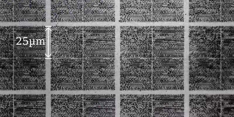
Did anyone else try reading the data off the picture? When I processed the image of the highlighted square, I got “We’ve been trying to reach you about your extended w#sgr!&?!” Obviously data integrity is not worked out yet.
The bits might be getting clobbered by JPEG compression or something, try to find a higher quality image. Great job decoding it anyhow!
To read or write this 2D WORM storage, one needs a full room of hardware. The density might be 6x more dense, it does not make it useful. DNA does way better.
It’s always cheaper when you can’t rewrite data…
And cheaper yet when you can’t read data…
The classic Write Only Memory https://en.wikipedia.org/wiki/Write-only_memory_(joke)
Well since it’s ceramics it could be good for long term storage, i.e. Library of Congress scanned can put on a cube could last thousands of years, unless somebody dropped it I suppose.
History repeating itself. For long lasting records ceramics have always been the go to medium.
If it ain’t broke…
Perhaps I am making a math error, but there is a 1.5TB microSD card. MicroSD cards are 11x15mm, so that must be very close to 1 TB per square centimeter of area unless I am misunderstanding how they are calculating that.
A nail file will get that microsd up to the same density. Might even be useable afterwards.
Samsung currently has a flash chip that is just slightly larger than 1cm2 and holds 1TB, so, this thing doesn’t seem very useful unless the long lifespan is important.
I wouldn’t be surprised if the actual dies could be much smaller still, since they keep stacking more layers.
I’d be much more interested in a new storage medium designed for reliability and longevity than one set up for maximum bytes per area.
Just like Beammos
http://www.rcaselectron.com/possin1975img.pdf
typo – Beamos
So what wavelength of laser are they using that is able to focus down to such a tiny spot required for this kind of data density?
Somebody check my math here, square root of 8 trillion bits, 2,828,427 on a side of a cm, 282842700 in a meter, 3.5355340618E−9 meters each spot, so, 3.5 nanometers? Seems optimistic for an optical laser. So, if it’s true that “3nm” is a marking term in the world of computer chips, then what voodoo is this? I read that electron beam can’t even do better than 10nm. Am I missing something? Oh also miles of forward error correction.
Did anybody actually decode the QR codes in the picture?
Your math is correct. Writing dots with 3 nm spacing is within the range of electron beam mask writers for the 5 nm node. The beam is 10 nm wide with a bell-shaped distribution and positional accuracy is around 0.1 nm. If the target ceramic coating reacts in a non-linear way to electron bombardment, structures smaller than the beam width can be created.
I’m pretty sure that they don’t do it with lasers, that would be like re-inventing the wheel. But try to explain electron beam nanolithography to potential customers and investors…
Your math is correct, which makes me doubt their claim of 1TB/cm^2 a lot, given that it appears in the picture to be closer to 1um^2 per bit, which is about 88,000 times larger. Unless they have some way of stacking 88 thousand layers and having it still work.
Put that big “fan” subwoofer in the server room and your data is gone!!
:) haha
Reminds me of another similar storage scam – called InPhase Technologies. They also promised reading holographic storage by a high-speed camera. Funny part was, that their leaflets had watermarked stock images – which they likely not bothered to license :D On the other hand, I actually own some of those high-speed camera boards, from a lucky eBay find.
128 bits in 25 um linear density = 5.1*10^6 bits/m. Which means an areal density of maximum 328 MB/cm^2. I guess they want to stack 3,000 layers per drive? The image didn’t pass the sniff test. I’m sure scaling down a laser and microscope combination by two orders of magnitude will be trivial though…
Still waiting for DNA data to be a thing
https://en.wikipedia.org/wiki/DNA_digital_data_storage
Youtube might have plenty of space but it’s write-speed is dire.
Chia farming?