You might remember that KiCad 7 came out this February, with a multitude of wonderful features. One of them was particularly exciting to see, and the KiCad newsletter even had an animated GIF to properly demo it – a feature called “Background Bitmaps”, which is the ability to add existing board images into your board editor, both front and back, and switch between them as you design the board. With it, you can draw traces, recreate the outline and place connectors over these images, giving you a way to quickly to reproduce everything on an existing PCB! I’ve seen some friends of mine use this feature, and recently, I’ve had a project come up that’s a perfect excuse for me to try it.
In short, something worth selling to a known tinkerer like me, but not particularly interesting otherwise. Nevertheless, about half a year later, when I fed it the desired 10.5 V from a lab PSU and gave the power button a few chances, it eventually booted up and shown me the BIOS menu on the screen! I’ve disassembled and reassembled it a few times, replaced the DC jack with an original one from a different Vaio ultrabook I happened to have parts from, and decided to try to bring it back to original condition.
In total, I’ve spent a good week (nitter) trying to make this Vaio work properly so I could make a portable typing machine out of it. Its Atom CPU with PowerVR graphics made it extremely hard to have a Linux distro boot, as everything i386 I tried would hang indefinitely after GRUB.
Lack of battery didn’t make the experience pleasant either. I wanted to build a new battery out of two smartphone cells in series and a salvaged protection board from a different Sony battery, but it turned out that Sony had an extra pin on the battery connector, going to a proprietary controller that was apparently specifically designed to prevent non-legit battery use.
At some point, while demoing this laptop and my battery circuitry journey to a friend, I accidentally connected the salvaged Sony BMS in reverse, which made the laptop release some magic smoke – it still boots up, but when it comes to making it work in the way it was originally intended to work, my hopes are gone.
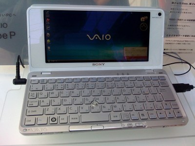
Despite everything, I love this laptop and don’t want to give up on it, even though I’ve never actually got to make use of it. It’s tiny in an adorable way yet with hardly any compromises in sight, it comfortably fits in purse-sized places, and it’s got some wacky aspects to it too, like the 1600 x 768 screen and a trackpoint in the middle of the keyboard. The main problem is the mainboard, sadly – it’s a work of art and engineering alike, but it just doesn’t work well in the world of today, and the missing parts that rely on proprietary interfaces make it a financially Sisyphean task to try and restore this laptop. Today, let’s peek inside a legendary Sony laptop from 2009, and then use KiCad’s new reverse-engineering features to take a dig at rebuilding its mainboard.
A Look Inside
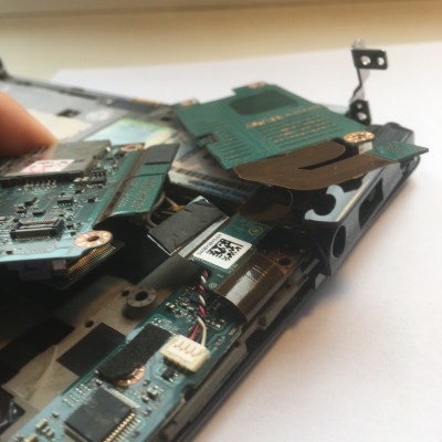
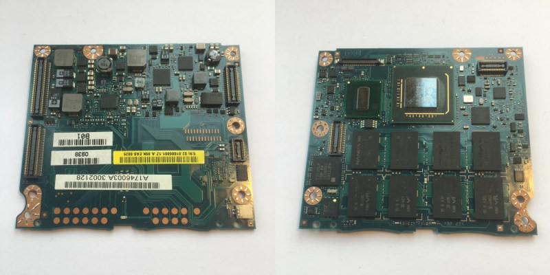
The innards of this laptop are an engineering marvel. A significant chunk of the laptop’s bottom half are taken up by the battery – the 1.8″ SATA HDD with its IDE-to-SATA on-FPC converter, the motherboard with the soldered-on CPU and RAM, the WiFi/GPS/BT expansion board, and the port PCBs take up only about 60% of the laptop’s inner space! Sony has made heavy use of flex PCBs, and not just that – half of the FR4 boards have flex layers in the middle of them! It’s a rare manufacturing technique to see in real-life boards, and this can’t have been cheap to produce.
All in all, it’s fascinating to look at just how well everything fits together inside of this laptop. If you’re interested to know more about what makes this laptop tick, someone on Hackaday Discord has linked this document to me, analyzing the hardware of this laptop – sadly, without pictures, but here’s a few to satiate your curiosity, and there’s also some wonderful teardowns!
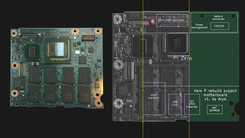
I’ve covered laptop motherboard reuse before, and building a new motherboard for an existing laptop is obviously going to have many parallels. Here’s the main aspect that gives me hope – we have schematics! I won’t share them here, but you can find them easily if you look up “Sony Vaio VGN-P Series (Foxconn MBX-187).pdf”. This alone is super helpful and in fact makes this rebuild possible, because the connectors on the board turned out to have some wacky pinouts. For instance, the LCD has a weird LVDS pinout, and unlike many others, doesn’t implement backlight on the LCD panel itself – instead, the backlight driver chip is on the motherboard, and what we get is bare LED connections; reverse-engineering this without the schematic would’ve been a daunting task.
It’s not just the pinouts, either – not any connector will fit all these FPCs mechanically, the suitable connectors have very specific part numbers. However, the schematic lists all of the connector part numbers that I could need! They might not have datasheets easily available, but I can buy them, and that’s what matters. I’ve ordered the connectors I need – specifically, I only need a few, since I’ll get rid of the RF expansion board too. The RF board, with its two mPCIe cards and IDE passthrough for the internal HDD, needs way too much PCIe and proprietary interfaces for me to bother, and the schematic doesn’t contain any info about the connectors found on the expansion board specifically, so it’s just wasted space in the end when I compare it to other things I could build into this laptop’s shell instead.
Now, I just need to build a new mainboard! A friend of mine has helped me along the way, by drawing a Kicad footprint for the LCD connector from a datasheet she found. Still, there’s a good few tricky tasks when building a new mainboard for such a laptop – you need to copy the outline, connector positioning, and then add enough circuitry to make the laptop do what you need it to do. Thankfully, Kicad’s new Board Bitmap integration makes it easy to take care of all the mechanical aspects, and let me show you just how well this works.
Perfection In, Perfection Out – A Scanner Will Help
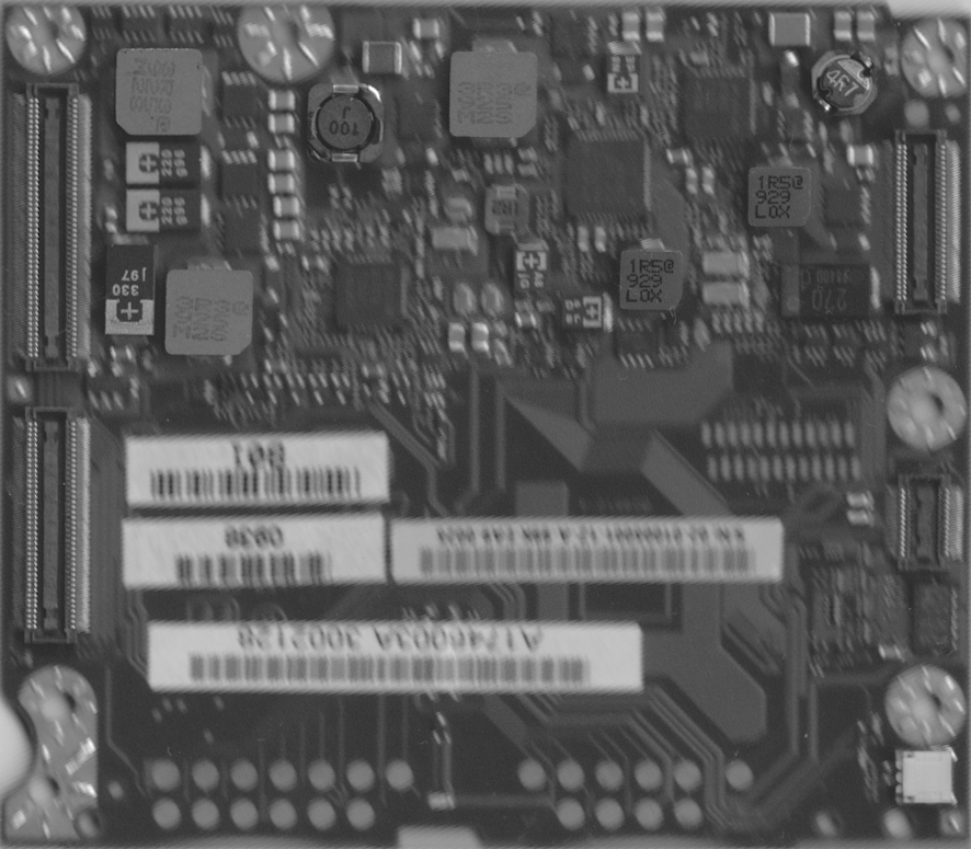
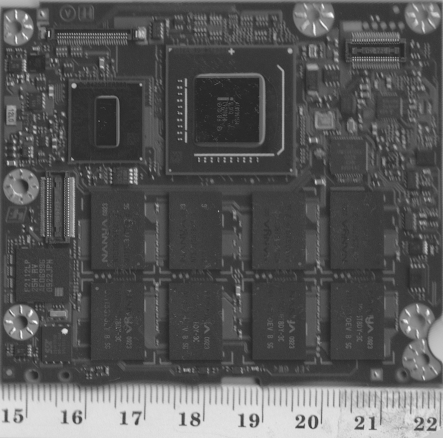
At the moment, the key to success is getting good pictures and processing them well. To get proper pictures, you’ll want to use something like a scanner – unless you find a way to position your phone just right, pictures from your phone will have a certain perspective to them, and unless you correct this perspective in something like GIMP, using these pictures will be a bother – KiCad doesn’t have a way to change perspective of an imported picture, so you have to do this externally. For scaling purposes, including a ruler is not a bad idea, because the distortion was negligible and was mostly a problem with screw holes where the shade produced by the scanner’s lightbar would have the hole position be slightly ambiguous.
Nevertheless, a scanner picture is what did the job for me, and I’ve talked to a friend who had problems with a phone-produced picture, so a scanner is what I’d recommend at the moment. I’ve heard that scanners can still have X/Y distortion, with slightly different PPI on X and Y axis, but I haven’t encountered that personally. I’m sure someone else has been using this KiCad feature for a while, though, and has found an even quicker solution than finding a scanner to put your board into – if that’s you, please do tell us more in the comment section!
I got some monochrome pictures at 300ppi, with negligible perspective differences, and these were more than enough. Of course, the board has components on it on both sides, and if they were just a bit taller or disproportionately placed, the board would’ve not been quite parallel with the scanner’s glass, which would’ve required me to actually change the perspective of the images in GIMP. If you’re scanning a board like that, desoldering connectors might be a solution.
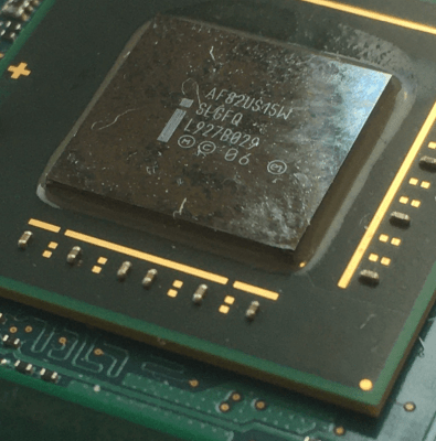
In my case, for a somewhat flat board, if I were to think this aspect through, I would’ve found a way to equally offset this board vertically relative to the glass while not letting any light in, adding some sort of standoffs and then a soft ‘frame’ of some sorts. Instead, I just pushed down on the scanner lid, which appears to have slightly cracked the chipset’s die on the scanner glass. That’s a disappointment, because I still wanted to power this board up a few times to sniff communications with things like the trackpoint, and now I’m not sure I can quite do that – but I will try regardless!
From Image To Wonderful Board
One Schroedinger’s chipset later, I got board images and cropped them in GIMP. It’s important that you rotate them so that the board is not off-angle in any perceivable way – if your PCB images are slightly rotated by a few degrees, you’ll want to tweak their rotation in GIMP/Paint/Kolourpaint/etc and re-import, because KiCad can’t help rotate them for you. Also, scanners will mirror your board image – so mirror it back as required, and, you can mirror images in KiCad.
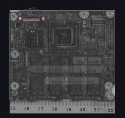 This is it! You’re ready to open the KiCad PCB Editor, press Place => Add Image, select your image and scale it. You’ll want to flip (hotkey F) the bottom image, but you’ll also want to open its properties (hotkey E) and change its layer from the default F.Cu to B.Cu – that’s how you get the images to change as you go from top to bottom layer while routing tracks. After all the rotating and cropping that I did, I was very pleasantly surprised when I scaled the image, placed my friend’s LCD connector footprint, and had it match perfectly with the connector pads on the image.
A bit of repositioning the images, and I’ve matched both the top and bottom outlines to a bounding box of the real-world PCB size, then redrawing the outline. I’ve also rounded the corners – the original board has sharp corners and they kept scraping at me as I was handling it! By the way, if you want to round corners of a board in KiCad, simply select both of the lines which make the corner, right click and press “Fillet Lines” – there’s no need to manually draw arcs anymore.
This isn’t a magic bullet for all your PCB reverse-engineering troubles, but it’s exceptionally useful – it saves you a ton of fiddling with calipers figuring out exact connector and hole positions! Load the images into KiCad, position them, and you can start placing your connectors and Edge.Cuts lines. With this method, you can reproduce proprietary boards in KiCad easier than ever before, as long as you can get a good picture – which is perfect for things like custom FPCs. Of course, it still helps if you can lasercut your board’s outline before submitting it for production!
It Will Only Get Better
There’s, of course, a few small caveats. For instance, when you’re drawing the outline on top of the images, it’s not hard to misclick and select the images, having them overlap the outline so you have to reach for the Esc key to continue drawing. This is very simple to solve, however – in the bottom right corner of the PCB Editor, in the Selection Editor field, uncheck “Drawings” and you won’t have that problem anymore. Overall, KiCad had support for different image scaling on X/Y, image rotation, or maybe even perspective tweaks, it’d be a bit quicker to start reverse-engineering any given board. At the moment, of course, reverse-engineering is not the main purpose of KiCad – but it will become more prominent!
Having this integration is a wonderful step forward for building all sorts of boards, and these quirks are no showstopper – they can’t even approach the immense value that this tool provides, and it’s a new addition so the quirks will be smoothed over. I’m only listing them so that you know what to expect at the moment, but in future releases, I’d expect background bitmaps to only become more comfortable to use.
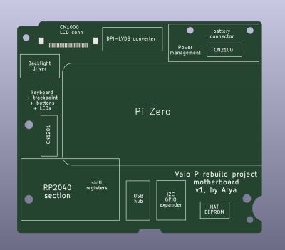
As for the Sony Vaio, I’m going to put a Pi Zero W onto this board and work on converting its DPI (parallel RGB) output into LVDS that the screen needs, and slap an RP2040 onto the board for keyboard/trackpoint/LED purposes – that should make for a good v1 board. If the LVDS part pans out, I can’t wait for the moment when this laptop is usable as my daily driver! Given how quickly I work on my projects, this one could take a year, but I’m seriously thankful for KiCad making quick work of previously the most annoying part of such reverse-engineering. In the meantime, the board pictured is on my GitHub.
I hope that this part of my journey can be a demonstration of how quickly you can reverse-engineer a PCB’s most important aspects with this new feature that KiCad 7 brought to us. Just like when we used KiCad’s then newly added SVG import to build a Jolly Wrencher SAO board, this is one more addition to your KiCad toolkit that you might not have known you needed!
Main/thumbnail picture made by [Wificable]!


Now do this with a HP Jornada 720.
no u ;-P I’ve described the method, it’s up to you to apply it!
On the other hand, the Jornadas are so thick, you could easily bodge everything in. I tried to find a usable screen for the Jornada 680 a fair bit ago, but couldn’t find one that would fit the lid…
Seems like a good opportunity to experiment with Pi CM4?
Yeah we’ve been thinking about that! For now, I just want to put a Zero 2 W onto there – I know it can be powered from a single LiIon cell efficiently, and its resources are more than enough for me. However, in the future, I could absolutely add a CM4 – though I’d rather someone else would do that, and, I’m open-sourcing everything anyway so that helps! Just, for my own goals, there’s not much that a CM4 would be good for here, that a humble Zero 2 W can’t provide.
Thanks for an interesting and well-written article.
However, with respect, that is not how the phrase “take a dig” is meant to be used.
https://idioms.thefreedictionary.com/take+a+dig+at+someone
Perhaps “…give rebuilding its mainboard a shot.” would be a better choice.
I’m rooting for you Runner!
Good luck making idioms universal and not local specific.
Thanks, anonymous coward on the Internet! I’m praying that you will one day get a personality and some friends to go with it! 🙏
Since she is writing in English, and the idiom she used is *always*, in *every* place English is spoken or written, used according to the link I posted (if it’s used at all), it’s already essentially universal. She simply mistook it’s meaning. She also, unlike you, took my comment in the spirit in which I intended it.
Please do the needful!
oh thank you, that indeed makes way more sense, will fix!
A nice idea! I remember them. There are realy cute little laptops. A joy to put your hands on.
But even at these days I sold mine because it was to slow.
Olaf
yes they’re so, so adorable! was very hard to accept that it can’t just function with the guts it currently has, it’s a labour of love all throughout. hope I can rid it of slowness and the proprietary aspects with this rebuild, I believe this laptop deserves way better.
They are! It’s not the same now that these little machines have been replaced with a touchscreen phone or tablet.
Why no cm4? They are readily available
Much easier to just use a ready made complete board (an RPI Zero, 3,4,5) I suspect than fiddle with a CM4 special connector and run the wires and other components in the base board. More of a keep it simple short term solution rather than a bigger long term project around the CM4.
Checking at a couple of sites I buy RPI stuff the CM4 boards are not ‘readily available’ . Most all are ‘notify me’.
apart from the reasons I’ve listed above (CM4 doesn’t give me anything extra that I would want in this project, and power management is hella easy with a Zero), soldering 42-44 pins on 2.54mm grid is way more attractive than soldering hundreds of pins with what was it, 0.5mm? 0.35mm pitch? That, and planning for extra thickness ain’t comfortable either. Might screw around and pull out HDMI, but that’s about it, I think! Plus, just, way cheaper and quicker to assemble board revisions during initial development, significantly so.
makes a lot of sense, thanks for the reply!
Target3001 has this feature since many years ago,I remember having good times scanning an el cheapo yellow multi meter,case included, to use the images to design an add-on PCB of a ESR meter,it fit perfect at the first try. Those where the times!
Ohhh that sounds wonderful, makes me wish I could see pictures or a writeup!
I have the later VPCP with the Z560 CPU which while it is capable of running Windows 10, is severely limited by the 2Gb RAM.
I’d love to upgrade the RAM to the max supported by the chipset (4Gb I think?) to make it that much more useable.
I wonder if it is kust a matter of swapping chips, or if there is some SPC chip or similar hiding somewhere too..
The RAM upgrade along with a replacement SSD would have that thing in my back pocket much more.
Tears of joy here.
I have two P11 and want to build a motherboard based on the CM4 which fits perfectly.
However I couldn’t get the video signal converted to the proprietary SVDO signal the display requires.
Now I learn the bus to the display is actually LVDS. Can’t wait to work on it again.
I have one of these myself, in full working order except for a dead battery. It’s actually somewhat usable and responsive with either Raspberry Pi Desktop or “good” old WinXP.
But I am watching this project with interest all the same… ;-)
available on aliexpress in two months
I wish there was a replacement motherboard with an AMD Z1 Extreme, would be a compact hacker machine.
However the screen was imo not that good, a matte 1920×920 screen or at least a modern 1600×768 screen would also be a nice upgrade.
Where to send suggestions for Chinese manufacturers? :)
Poulsbo/GMA500 is cursed garbage. No Linux drivers that ever worked right and Windows drivers were dumpster fire (that was based on the Linux driver stack to begin with).
I messed around a lot with Aigo MID back in the day.
Also, if anyone wants some pain for almost free, there are brand new ITELCO IDOL’s on eBay for cheap on eBay right now. I managed to install XP on one, but BIOS is a nightmare and I cannot get keyboard map right.
Having said that VAIO P form factor and Sony design is great, the guts are just garbage.
I swear U1/U3 with Transmeta was more fun despite being slower.
I have a gen 2 Vaio P that I love. I recently pulled it out and set it up with AntiX linux and use a remote x2go session for most of my actual stuff since it’s so slow and the GMA500 is next to useless. The keyboard is one of the better keyboards ever shipped on a UMPC (imo).
I have thought of doing something similar to this but probably a while down the pipeline. Love seeing there’s others out there showing these machines some love, especially since the hardware that shipped in them originally is so bad, even by the standards of when they originally shipped.
This would be sweet, as the form factor of these machines is perfect, but guts re-arrangement is challenging, to say the least. Meanwhile, I’ll leave a pro tip here: if you have an old vaio p, get a QC3.0 usb trigger with a tip for DC. These output 12 v, which Vaio P happily takes. This makes the machine untethered from ac adapters and portable again. Looking forward to this project development.
It’s a shame I can’t find one of these for anything less than overpriced, unique doesn’t mean good.
I have a vio vpg. N100 CPU, good battery, win 7. Would love to upgrade the CPU. I don’t have the engineering knowledge to do it. Bummer.
Amazing! I would love to breathe new life into my old Vaio P, turn it back into a more usable portable carry. Unfortunately I’m just a programmer, with basic understanding of PCBs. Wish I could help/work on projects like this one.
I bought one of these with the same project in mind, without realising how far out of my league it was… but now that you’re working on it I think I can definitely follow your instructions through it !
Have you jumped in to try it yet?
Where is this project at in 2026? Hopeful some magic can be weaved for these Lil Ps
I would like to see more on it if it’s available.