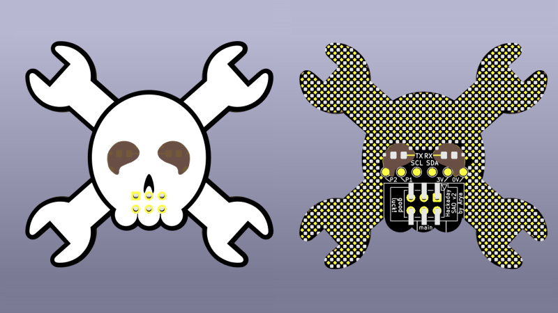
If you plan to attend Supercon or some other hacker conference, know that you’re going to get a badge with a SAO (Simple Add-On) connector, a 4-pin or 6-pin connector that you can plug an addon board onto. There’s myriads of SAOs to choose from, and if you ever felt like your choice paralysis wasn’t intense enough, now you have the option of getting a Jolly Wrencher SAO board!
This board gives you an SMD prototyping space, with 1.27mm (0.05″ pitch) pads, suitable for many passive components, ICs and even modules like the ESP32 WROOM. Those pads are diagonally interspersed with ground-fill-connected pads – if you want to bodge something on the spot, you don’t need to pull separate GND wires. Given the Supercon badge specifics, the SAO-standard SDA and SCL pins have RX and TX labels as well. For bonus points, the eyes are transparent, with LED footprints behind them – it’s my first time designing a PCB where the LED shines through the FR4, and I hope that the aesthetics work out!
This design is open with gerber files available for download, so if you thought of making a quick PCB order, I’m giving you one more .zip file to add to it. Otherwise, it’s possible that you will find a Wrencher board lying around at Supercon! Now, I’d like to tell you how KiCad 6 made it super easy to design this PCB – after all, there’s never enough SAOs, and it’s quite likely you’ll want to design your own special SAO, too.
Pleasant Surprise
I started with an SVG of a Jolly Wrencher that I found online. My first experience with importing outlines into KiCad, back in KiCad 4 days, required tinkering with DXF import formats – even putting things through LibreCAD to make it import smoothly. While I expected some improvements, I was ready for rough edges to show up.
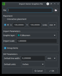 However, when I opened the PCB editor, I didn’t see the “Import=>DXF File” entry that I used last time. Instead, I noticed that it’s been changed to “Import=>Graphics”. When I opened it, I was greeted with a simple menu titled “Import Vector Graphics File”, not a DXF-specific option in sight – a reassuring view. Would it be possible to actually import SVG files natively? I clicked the “Select file” button.
The SVG file of the Jolly Wrencher was visible in the file picker list, and in the lower right corner, “SVG” and “DXF” both appeared in the supported file type dropdown. I picked for it to appear on the front silkscreen layer, and when I clicked OK, the Jolly Wrencher polygon just appeared on the silkscreen in the PCB viewer. Apparently, this option has been added in KiCad 6 – the version just released this year, and I’m excited about what this means for our board designs.
For a start, such straightforward import of SVGs makes it way easier to import logos, art and other graphics. You don’t have to go the bitmap2component route anymore, or use SVG2Shenzhen. While both of these are powerful tools, a built-in SVG import tool that will put your logo on any layer you pick has way more potential, purely because of how easy and quick it is to use. This import option lets you put all sorts of artwork on your board straight from our favourite image editor, without having to add a footprint library or deal with other sorts of limitations.
Furthermore, it also makes mechanical design easier if you want to export your artwork’s contour as board outline. To create an outline for the SAO, I selected the Wrencher SVG elements in Inkscape, then pressed Path=>Outset a couple of times, making each individual element of the Wrencher larger. Then, I selected Path=>Union, joining all elements together into a usable outline. The eyes and nose remained inside the contour, but a Path=>Break Apart click (Ctrl+Shift+K) made them into separate paths, promptly removed.
I saved the resulting outline as a separate file, and then imported it onto the Edge.Cuts layer. Just like that, the Wrencher SAO was ready. Making your own badge or SAO from an SVG is legitimately this simple in KiCad 6, and only requires tools you already likely have installed.


If It’s This Simple, I’ll Make It Complicated
Of course, after the initial excitement, I came up with extra requirements, allegedly to make this SAO even better, but also because I wanted to play with the import process. With the default 1.0000 import scale, the badge size was about 8 cm x 8 cm – too large for an average SAO, and definitely too large compared to the Supercon badge. In the end, I settled on 0,6000, which resulted in both X and Y dimensions being just under 5 cm – a comfortable size for a SAO. Some PCB fabs have price breaks if the board doesn’t fit in a 5 cm x 5cm square, so I hope this helps you during ordering. I didn’t find a “measure the PCB boundary box” setting in KiCad, but the measuring tool (Ctrl+Shift+M) helped. This was easy.
If you design a PCB to be worn on the body, it’s important that you remove sharp corners from it – the corners will catch on clothing and other things, and possibly injure the wearer. For the Jolly Wrencher, this means the wrench corners must be rounded, unless I wanted the PCB to double as a weapon – wasn’t on my wishlist. The rounded corners are an acceptable aesthetic compromise, and you aren’t gonna be unscrewing any nuts with this board anyway – unless I somehow got lucky with the dimensions!
This meant I needed a way to round corners in Inkscape. Quick search has shown that Inkscape has a built-in filter for this – but only if your Inkscape install is new enough. On my Ubuntu 20.04 LTS, it wasn’t, and I decided to use the Snap-provided version instead – given that one of Snap’s stated purposes is delivering new software to our desktops. My Snap experience hasn’t been smooth sailing, but I’ve benefited from it here and there. It appears, however, that the Snap-packaged version of Inkscape is unable to open .svg files – I opened the file picker, and couldn’t see any SVG files appear, “Open With” didn’t work either.
This is a sandboxing bug, of course, springing up in various forms from as far as 2018. Snap developers blame Inkscape developers for not using the correct declaration in their Snap manifest file. From my experience, if you’re developing a sandboxing solution meant to be used by thousands of desktop apps, each backed by a huge userbase, it’s your responsibility to make sandboxing parameters crystal clear and impossible to screw up in such a major way – it won’t work out otherwise. Which is to say, I eagerly await the Year Of Snap On The Linux Desktop – perhaps, sometime next decade. In the meantime, the Inkscape PPAs works without a hitch.
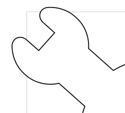 The “Corners (Fillet/Chamfer)” option finally became available in the Path Effects menu. I could fillet each of the four wrenches completely, but I specifically wanted to preserve all sharp corners except the two that stick out. The way I went about it turned out to be complicated and took an hour or two to figure out, since I wanted a perfect radius fillet for all eight corners, and ended up splitting each of the wrench ends into separate paths, filleting them and then re-joining. There’s a “Change only selected nodes” setting in the Corners tool, but it’s not clear how to make it work, hence the splitting. If you’re fine with a quick and dirty rounded corners, follow this tutorial instead.
After filleting the Wrencher, I regenerated the outline using Outset and Union tools again, so that the outline fillet radius would be neatly concentric with the silkscreen fillet. Saving the silkscreen-intended and the outline-intended parts as separate SVGs, I imported them onto their respective layers, moved them on a sub-millimeter grid until they matched visually, and the aesthetic part of the badge was ready.
An Experimental Protospace
 I’m a big fan of deadbug prototyping – if it were up to me, every soldering iron would be sold with a roll of 0.1 mm enameled wire. I also didn’t want to add specific-purpose-aimed components to this badge – ideally, you would only actually need 4 pin headers, as these are easy to source anywhere. I decided to fill the backside of the board with SMD prototyping pads, letting people add their own components – after all, the most fun components tend to be SMD. The idea that it should be possible to prototype Supercon SAO additions and tools on the spot – with inspiration taken from the 2018 Supercon ESP32 addon by [morgan] and the BornHack 2021 badge.
If you fancy some THT, you can mod the PCB files, make one of the wrench ends a THT protospace and order the boards modded in such a way, but I decided to have the front of the badge be as clean as possible by default. This protospace has 1.27mm (0.05″) grid, and should be compatible with SO/SOIC ICs, and castellated modules like the ESP32. One thing I hope for is that these pads are actually large enough to be reliably soldered to – until my own PCB shipment arrives, I can’t quite verify that. I apologize in advance if the protospace pitch turns out way too intense for your own skills, and I hope that the equipment available at Supercon will compensate for that!
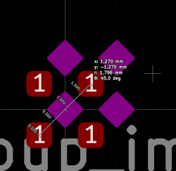
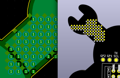 I initially wanted to go with metric grid on one of the Jolly Wrencher’s wrench ends, but decided against it. There don’t seem to be many parts that use metric grid for their pins, thankfully. I had to make the pads large enough to seem usable, but small enough that the ground fill would be able to get in between the pads, and I added mask openings to the footprint while at it. Once the ground fill worked, I copy-pasted it all over the board with grid set to 0.025″ so that I could quickly align the pads properly. Setting your grid to a certain size when placing footprints helps implement such ideas at a rapid pace!
I haven’t found a better way to build flexible protospace footprints in KiCad, but I’m all ears! In general, there seems to be two ways to make prototyping spaces in KiCad – either create the entire space as a separate footprint and plop it on your board, or split it into grid-align-able smaller protospace pieces that you stack together; the latter option is way more convenient for arbitrary shape boards like this one.
Components And Keepouts
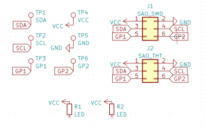
Of course, I had to add components like the 6-pin headers and testpoints. You’ll have to decide which parts of the badge you want to keep in the schematic. My observation is that things which carry specific signals, like connectors and testpoints, are best done through the usual “symbol => footprint” route, while things like protospaces and artwork are best done as standalone footprints or even just imported graphics. Remember to make sure that the “Delete footprints with no symbols” option is unchecked in the “Update PCB from Schematic” dialog if you don’t want to lose your artwork on schematic sync – thankfully, that seems to be the default.
Our editor suggested that I add LEDs behind the eyes, and I decided to go the “SMD LED shining through FR4” route to avoid through-holes. While THT LEDs have their charm and benefits, I imagined they’d look a bit off, and SMD LEDs are ubiquitous. Two 0805 footprints did the job, and using the “Handsoldering” variant should enable you to use 0603 with ease. I didn’t add resistor footprints – instead, I positioned the LEDs so that adding a resistor to jumper their cathodes to one of the numerous ground fill pads around would be trivial.
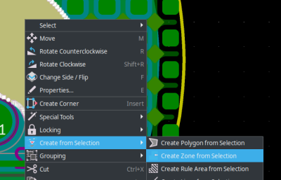 Making the eye sections transparent meant I had to remove the ground fill from the bottom layer specifically where the eyes are – the way to do this in KiCad is a keepout polygon. I initially dreaded this route, since I thought I would need to manually trace both of the eye shapes – turns out, you’re able to import the eye shapes onto any layer in KiCad, right click them and use the “Create From Selection => Create Zone From Selection” tool in the right click menu. With that, in no time, I added eye-shaped ground fill keepouts, then imported the same eye shape SVG onto both mask layers, and the eye region of the board became transparent – as much as bare FR4 is transparent, anyway.
This ability is wonderful and helps with many things; in part, it means you can add filled zones from SVG contours – simply importing your vector onto a .Cu layer can be suboptimal when you want the resulting shape of copper to be connected to one of the nets on your board. For instance, if you want to make a custom capacitive touch slider, you can just design it in Inkscape, import the SVG onto your board and turn the pads into copper zones.
Random Encounters
After submitting these boards to JLCPCB, I got an email from their reviewer. Her email said: “boards covered with many pads should be made with ENIG according to company process”. I wasn’t interested in the associated price hike going from HASL to ENIG, and decided to ask what the specific problem was. She replied that, given the amount of pads, short-circuits might appear – which makes sense, given how HASL works. The implication I felt was that they didn’t want to put extra effort cleaning those up – which sounds fair to me. I asked them to produce the board with HASL and that I wouldn’t raise complaints about short-circuits – and surprisingly, they agreed to this. I’ll see how my boards look once they arrive – it will be an interesting test!
 Half a day after ordering these boards from JLCPCB, a friend on the Hackaday Discord pointed out that on either side, there’s nowhere for the silkscreen-placed order number to go – something that’s a JLCPCB requirement unless you pay a small extra fee to waive it. JLCPCB lets you download and inspect PCB files after production changes have been made to them, an option I promptly turned to. There, I found out that they put the order number in the tiny space they could find behind the through-hole SAO connector outline – a pleasant surprise. I recommend you pay a bit for the “remove order number” option nonetheless, it’s a small price and guarantees that your badge won’t end up with Y23-84112 front and center on the silkscreen.
I have an affinity towards the “^__^” emoticon, so I decided to make silkscreen patch SVGs, turning the badge eyes into two ^ shapes. That way, I could just place them onto the original silkscreen and regenerate the gerbers. This turned out to be surprisingly hard somehow – after I had drawn it, the shapes wouldn’t import as a filled polygon and instead would import as two contours. The trick that worked in the end was using the “Stroke and Fill” toolkit in Inkscape, filling the outer shape black and the inner shape white. I have no idea why that helped, but I hope it helps you too if you ever encounter this problem, and the ^ patch files are in the repo for your tinkering purposes.
It’s Way Simpler To Make A Pretty PCB
You can design SAOs and artsy PCBs of pretty much arbitrary art complexity in this way – or perhaps, simply put your logo/artwork/entire schematic on the silkscreen. The more artistic you make your PCB, the more I suspect that tools like SVG2Shenzhen will make it easier for you. I have never gone through the SVG2Shenzhen process, but I suspect that projects like the MCH2022 badge would benefit from the automation involved. That said, it’s also wonderful that all of our simple PCBs now have a straightforward and efficient route available to them.
You don’t have to do most of these steps I described! 80% of what made the Jolly Wrencher PCB cool, was completed nine paragraphs into this article – the remaining part of this article shows you how to apply further polish. Any of us who has designed enough PCBs, knows – you can spend an inordinate amount of hours on making a PCB even more perfect than it already is. I certainly had my share of fun as I was layering requirements on and on, and I hope I have shown you just how easy it is to have fun in KiCad 6.


Thank you for coming up with a more mature attribution for the SAO acronym – the original choice took me back to the playground, and always rather grated.
Mature, or prudish?
Not in the least bit prudish – it was just being vulgar for the sake of it, there was no wit or wisdom in calling it a ‘shitty add on’, but each to his own.
Nah, it’s Sword Art Online and it will be that way for a LONG time.
Hahaha, I get that reference. Every time I’d look for “SAO” on Google, most of the results were for Sword Art Online :D
Here in Oz a SAO is a well-known biscuit (more of a cracker really) that’s been around for over 100 years.
https://en.wikipedia.org/wiki/SAO_(biscuit)
“Some PCB fabs have price breaks if the board doesn’t fit in a 5 cm x 5cm square” — *Doesn’t fit*– Or *does fit* ??
There is a price break, no matter which way you are going!
Err, looks like I have always misunderstood “price break” – I thought it meant break as in discontinuity, but apparently it means a discount.. live and learn!
Yes, usually means ‘discount’, which is why I was confused…. You’d think if the board were smaller, it’d be cheaper– Not the other way around as expressed here.
After Superdupertrupercon, will these be available on Tindie?
So, after the scaling, are the wrenches metric? ;)
dont forget filleting the inside corners as well… unless your board house has a 0mm router bit ;)
I bought a box of those drill bits on Aliexpress, but for various reasons it is impossible to chuck them properly into the drill press!
Nice roundup of your design procedure, well written. I am also pleased of the new import an export features offered by KiCAD 6.
One comment on the boundary box dimensions you were missing: if you add the “board characteristics” (to be found in the place menu), it will tell you the “board overall dimensions”.
You don’t need to place the board characteristics table to get the dimensions/area of the board – just open the board statistics dialog from the Inspect menu, and it will give the X and Y dimension for the board’s bounding box along with the actual area the board outline uses in that rectangle (with the option to include/exclude the holes in that area).
It would be fun to have one LED-eye hooked up to the TX, and one to RX :)