So far, I’ve talked about why DisplayPort is the future, introduced the basics of how to work with it on the hacker level, took apart and tamed the DisplayPort altmode, and recently, went through the eDP (embedded DisplayPort) display technology. This time, I want to give you a project library to reference, so that your hacking goes as smoothly as possible – real-world examples of open-source DisplayPort boards, a few boards I’ve worked on, part numbers, and whatever other information you might need.
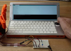
Over the past few years, I’ve noticed that a non-zero amount of cyberdeck builders buy eDP screens with HDMI converter boards on Aliexpress, then connect them to SBCs using USB-C to HDMI adapters, or ignore the onboard eDP port; even this super cool Framework-based cyberdeck has done that! I get that it’s the simplest option, but I do believe that you ought to know how to improve it. The issue is that this double-conversion decreases the battery life significantly by burning two extra ASICs doing video conversion back and forth. Every hour of battery life matters in a cyberdeck, doubly so if it’s based on a low-power device already – you could easily cut your battery life in half if you’re not careful!
With these projects and references in your arsenal, my aim is that DisplayPort becomes way more comfortable for you to work with. Thankfully, there are quite a few projects to reference by now – let’s delve in.
Right out of the gate – are you looking for an SBC with DisplayPort support? The BoardDB website, a database of single-board computers, has a DisplayPort filter – click this link with the filter already enabled and browse through.
Gateway Tablets
Perhaps the most omnipresent open-source DisplayPort project is the Adafruit adapter for iPad Retina displays. When iPad Retina displays became available to hackers, as far as I can tell, it was [Andrzej] who discovered that they were using the eDP interface, and figured out that you could easily convert it to DisplayPort. Eventually, that led to Adafruit making an adapter board they could mass-produce – which is one of the best outcomes for such an idea! We’ve seen proprietary boards for these displays being sold since then, even with USB-C DP altmode support – but the Adafruit board is open-source, which makes for a way better start, more so given they have cool tutorials to go with it.
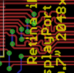
There’s many things you can learn from this board, and some things you shouldn’t. Well, one thing you shouldn’t – the trace routing on the Adafruit board is seriously puzzling, even though it undeniably works. However, it gives you an example on how to drive a bare backlight – something you still might have to do when it comes to tablet displays. Oh, and there’s an ATTiny for managing the PWM input of the backlight driver, and a few buttons – if you’re making your own eDP adapter and you need a backlight driver controller, you could do worse than yanking their ATTiny firmware and schematic.
Now, this has kickstarted a fair bit more eDP hacking – like this Retina adapter we’ve covered a few years ago, there’s been other boards for other eDP displays, too; and, iPad screens are still here and available for purchase. The bottom line is that wiring up an eDP display is easy, and it might make your cyberdeck all that more practical. Now, a Raspberry Pi with a DisplayPort connection would be awesome to have, but I suppose RPF’s allegiance to Broadcom’s allegiance to HDMI makes it unlikely – until someone figures out an accessible and Pi-compatible DSI-DP converter, or at least, I can dream.
Laptop Panel Handling And Connectors
Here’s something I no longer have to dream about – an adapter from DisplayPort to different eDP connectors, that [WifiCable] and I have recently designed. Remember – eDP displays only use two different connectors, and, there’s an abundance of FPC-to-eDP cables on Aliexpress and other Eastern marketplaces, so you might only need to add an FFC connector onto your board. As for pinouts, this adapter supports four different eDP pinouts with three connectors, including the pinout of the Asus ROG Ally display, and it handles touch-enabled displays too.
 Since the DP signal goes to three connectors at once, there’s some suboptimal stubs involved, but it’s an experimental enough board that I’m not particularly worried. The capacitors are added inline, but can be bypassed with 0 Ω jumpers if you so desire – as I’ve been saying, footprints are free. And, this board is currently untested – we’ve only just ordered it and will be assembling it within like a month. That said, I’m open-sourcing it now – it has enough work put in that it’ll already be useful. Also, in the near future, I plan to convert the DisplayPort socket to a USB-C port with DP altmode support, and use the existing USB-C socket for charging input – that will be a fun adventure!
From this board’s files, you can get things like the eDP panel pinouts you can copy-paste into your KiCad project, as well as footprint and symbol for a DisplayPort connector. Now, to be clear, we got the footprint and symbol from LCSC. You can find DisplayPort sockets on Mouser and Digikey, but LCSC is that much cheaper.
Actually locating DisplayPort parts on LCSC is tricky, but gets way easier after you follow some simple rules. First rule is – don’t only check the DisplayPort category, since manufacturers seem to often ignore it; check the D-Sub/VGA connector category, too. Second rule is – do not touch absolutely any filters, make sure all of them are disabled – you have to do this because filters on LCSC are deeply broken; the only thing you can touch is “In Stock”, so only check that. Third rule is – set “items per page” to 100, for your own sanity’s sake. Maybe complain to them so that they bring back the 500 option, because I’m personally tired of doing that, only for them to again limit it back to 100 a month later.
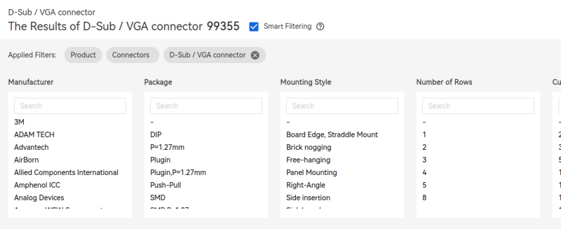
Also, here’s a DisplayPort socket on LCSC, and another, and another, and here’s a miniDisplayPort socket; please don’t buy them all out, thanks. There’s no shortage of chips either, just that they can be a bit tricky to find. For instance, do you want high-speed muxes? Here’s two independent KiCad projects who do DisplayPort “one port to many ports” KVM-style muxing; this one just does DP and this one also supports USB. It’s no MST, but if you want to switch between screens or DisplayPort sources, it’s a pretty viable solution! In general, if you look up "AUX+" kicad in the GitHub search bar, you can find out about some fun boards, and even find ICs you might’ve otherwise missed.
As an aside, if your DP transmitter does DP++, the MXM immobilizer project from [WifiCable] gives you a reference implementation that supports both DisplayPort and HDMI/DVI backwards compatibility mode on your connector. This one has been taken from working laptop schematics; that said, this design hasn’t been tested. This PCIe-MXM design was tested, though, and even though the license is super restrictive, you should still be able to check schematics, especially if you go to the commit before the author deleted the KiCad port of this adapter.
USB-C DP Altmode And Motherboard Hacking
Here’s another design you can make use of: a USB-C to eDP converter. I’ve recently been finishing bringup of this board, and while I got a little stuck on making the firmware perfect before making it actually work, the AUX connection has indeed after bodging two resistors onto it, which are now integrated into the design. The only area yet unexplored are the main DP lanes, which, I’m sure, have no problems at all and will work wonderfully first try as soon as I figure out the right VDM (edit: I have since done more adapter bringup work and realized I’ve mixed up the main lanes, a fix has already been pushed to the repo). I’ve partially covered this design in the Altmode Taming article and talked some about DisplayPort USB-C muxes, but I haven’t published it yet at that point, and that was long overdue, so here you go.
 Really, the main things you can borrow from here is the mux implementation, and USB-C to DisplayPort routing if you’re fancy. However, there’s also the connector being used – it’s a nice one. If the connector doesn’t look familiar, that’s because it’s the connector used on the Framework laptop, for the KVM conversion mode that I’ve been working on. The Framework’s eDP connector is overall pretty capable – four lanes *and* touchscreen connection, all within just 40 pins! It’s capable enough that even system76’s Virgo, a WIP open-source laptop design, appears to use it; that said, they’ve confused the polarity because of Framework’s initially confusing data, so I hope they take note of this whenever they resume work.
This connector may look tricky to solder onto your board, what’s with the pads being fully hidden, and it is tricky to both solder and repair, but it’s a pretty suitable choice if you are decent at stenciling. Also, thanks to Framework as of recently, you can buy their cables separately– they’re locked into the 40-pin high-res pinout and you can’t easily change that, but you could definitely add an adapter if needed. If you’re looking for a fancy connector that still supports more hobbyist-oriented soldering methods, however, a good middle ground is using the I-PEX connector that eDP laptop displays themselves use, and then finding a male-male cable with microcoax wires on either Aliexpress or Digikey.
Framework’s connector is the connector you will want to use if you want to connect an arbitrary display to a Framework mainboard, too, and it’s not easy to make custom cables for it. That’s not an uncommon situation – some of the SBCs with DisplayPort in the SBC database list I’ve linked, will too have it on a connector that ain’t easy to work with; watch out! Fortunately, even here, you could use the Framework’s cable, plug it into the Framework motherboard, and put an I-PEX 40-pin high-res pinout socket on your adapter board – that’s what I’m currently doing for a small and yet-unfinished project of mine. Otherwise, if you need the touchscreen signals that Framework cable doesn’t pass through, you could do a breakout with a male-male cable; as long as you’re okay spending $50 on a cable, that is.
DisplayPort is not always faultless – for instance, you might find out that your SBC’s DisplayPort driver has not been tested with lane widths less than four, as [Timon] found out during the [Damn Linux Tablet] project. Nevertheless, if you connect a random eDP display to a random eDP device, due to the auto-discovery mechanism over AUX being a link requirement, it’s highly likely to just work – as opposed to the old LVDS days; and, making hardware for DisplayPort is seriously easy.
Capacitors, Resistors, And PDFs
When you see some of the open-source boards, you might see series capacitors, perhaps, even pullup or pulldown resistors on the AUX line, too. They’re something I ought to have expanded upon in the Under The Hood installment, but the second best time is to do it now, before the boards might leave you confused. An official DisplayPort spec will help with both of these – you can find it easily enough by looking up DP-1.2.pdf; I couldn’t find higher version specs PDF names for you since they’re not public. There’s no spec for embedded DisplayPort that I could find, and it’d be wonderful to take a look, so if someone has it handy, please do let me know!
You need series capacitors for both the AUX link (1.2 spec page 329) and the main link pairs (page 362); range is 75 to 200 nF, so regular 100 nF will do. The 0402 package is preferred, but 0603 is possible. Main link capacitors are only required on transmitter (source = upstream) end, but you can put them on the receiver (sink = downstream) end too if you’d like. Remember that stacking capacitors in series causes the overall capacitance to decrease in the same exact way that resistance decreases when you stack resistors in parallel, so you might not want to overdo it.
The AUX channel is a differential pair – as you might remember, it’s used for monitor parameter querying, link training, configuration, and things like audio. Just like USB2, it’s pseudodifferential – there’s resistors that sometimes have to be used for your device to be detected, or for the bus to be properly biased to work. The transmitter pulls AUX+ down and AUX- up to 3.3V, the receiver pulls AUX- up and AUX+ down. Oh, and remember HPD? It needs a 100k-ish pulldown on the device side (page 327).
Do you need either capacitors or resistors for a regular DP adapter? Likely not – a DisplayPort source will integrate them, and your display might, too. However, they might be useful if you’re working on a USB-C adapter or adding muxes to the equation, and it helps to know that they’re sometimes required.
All in all, DisplayPort is a great option for your displays, and it’s one you deserve to be able to work with – there’s no shortage of DisplayPort hardware around us. May these designs and references help you in your own DisplayPort forays, no matter what you might be building.
I thank [WifiCable] for help in compiling the materials and links for this article!


Comprehensive Article. Unfortunately there are no cheap DP capture solutions, or are there? Probably adapting to HDMI is the cheapest way.
On a slightly related note, I recently (ab)used cheap ($8) USB 3.0 HDMI capture dongles together with a small Tang nano FPGA board to shovel 180 MB/s arbitrary data into a PC, and even used that to build a small SDR prototype with 90 MHz bandwidth. I gave a talk about it at OsmoDevCon in case anyone is interested:
https://steve-m.de/projects/osmodevcon24_hsdaoh.mp4
https://github.com/steve-m/hsdaoh
yeah my hunch is that adapting to HDMI is indeed cheapest&easiest at this point in time – and, oh that’s an awesome project! noted, thank you for sharing ^_^
Amazing project! Would deserve an article here an HAD…
Outstanding work!
I had independently ended up actually implementing a HDMI out port on a ice40 based PCB (part of a data capture system for my job), mostly because HDMI just makes good sense as a good way to physically link a couple PCBs a short distance apart with reasonably fast synchronous serial. I was intending to design a separate board to ‘receive’ what would have just been more or less SPI over LVDS.
But then the thought occurred of perhaps just exploiting a COTS USB3 HDMI grabber like this, which seemed like a good solution, with only the ‘cost’ of complying to the DVI formatting so the grabber IC would be happy. Great to see it works!
I will likely have a go at seeing if I can get it to work on my board using the ice40hx8k chip (which has totally complete open source toolchain support, so good in fact you can do things like change the initial boot contents of RAMs in an image without recompiling it. ).
The only other observation that seemed to be missing from your presentation at the beginning => Implementing a PCIe endpoint in FOSS FPGA on an FPGA. AFAICT, this is doable with the Lattice ecp5g FPGA’s, some of which have the gigabit transceiver blocks.
There are some older Lattice Dev kit around, which were relatively cheap depite having pcie on the edge like a video card. These I acquired but never used because of the nasty self-destruct timebomb ‘trial’ licensing that then demanded about a $10k/yr license to run PCIe. Most all pci-supporting FPGA dev boards start at about $1k, and you end up getting that nasty $10k/yr / seat license fee.
But a PCIe endpoint board could be made to work with FOSS supported FPGA’s, at least for the slower link speeds. And this should work on a linux system then enabling the next step up in FPGA data streaming IO.
Until then, hsdaoh is a step better than yet another FX2 fifo implementation (you don’t mention it, but an additional *massive* problem with that ~45MB/s USB 2.0 HiSpeed is that it comes free with randome no-flow glitches depending on what the kernel is doing – there’s no FSM keeping the data flowing, so you very often get stalls for a few ms – and this means you need a 8+ MB deep fifo to tolerate that (my board above has a fx2 on it, and just adds a 32MiB hyperRam IC for that duty).
The real ‘streaming data capture stress’ test is to generate data with a counter in your FPGA at a fixed data rate, just a big integer overflow incremented steadily (as you are doing for your idle counter), then stream this to a file on disk, using an external drive or NAS array, and run it until you have filled ~10+TB. You can reconfigure this rate to test at different capture rates, but the trick is with that file you can quickly check the phase of the count to detect whether any packets or frames went missing: phase jumps in the count tell you how big the missing block is, and you can run a binary search, since you can calculate what the phase ought to be, and it’s unlikely for repeated data loss to *just so happen* to result in complete accumulated loss of exactly one bit binary counter overflow.
This lets you ensure the data capture chain (FPGA FSM at arbitrary rate to file) is reliable out to the timescale you might need. Alternatively it shows up what the MTBF is for the setup. It pays to use a NAS using ZFS to hold that file (because things like RAID have failure rates of every few TB, and ZFS is expressly designed to handle big data like this perfectly).
My ‘application’ for this reliable datastreaming is high-resolution ‘black box’ data logging, typically multiple analogue input channels monitoring pressure, strain, voltage or current transducers on high power experimental mechatronic equipment. These records let you reconstruct the chain of failure should such occur, and basically make it possible to learn from such failures, often due to unexpected conditions due to complex fluid rheology which are hard to simulate accurately.
Having the reliable data recording allows you go go back over a several-day long experimental run, yet ‘zoom in’ to the ‘bullet motion’ timescale right on the one event before everything broke. Can’t do that if the data is only recorded ‘if triggered’ which is how all oscilloscopes work: It just means they never save the one moment you really needed recorded.
After an experience where equipment failed without useful recorded data, you soon realize that using a ‘triggered’ recorder (DSO) is in fact a way to succum to ‘cherry picking’ your data, just in an automated way rather than by hand: You’re trying to decide the worth of saving the data, without doing so after the fact whilst looking over *all* the data: So you’re not doing science anymore, just trying random things and hoping to make progress brute-force. You can’t control what you can’t record.
You need to record reliably, and then select contiguous segments of data record for analysis where the behaviour is ‘stationary’, i.e., the cyclic operation of the device under test is repeatable. You can then determine whether it really is cyclically stationary, or not, and if not – determine the wear rate and lifespan of the equipment.
You can also do RFI noise analysis on such data, especially where saved data has a VHF sample rate, where you can do SDR on the residual noise from radio interference, then decode the local radio station and/or mains harmonic interference to use to verify the location/time the recording was taken. This is a way to verify the recorded data was indeed unlikely to have been falsified, and to verify it also hasn’t been rearranged such as being reordered.
The latter feature of ‘baked in verification’ is only really important for projects producing extraordinary results, specifically demonstration of potentially pivitol novel energy technlogies such as low-energy nuclear reactions and room-temperature superconductors, where charlatans have historically operated to fraudulently collect funding.
But the ability to just start recording, then run for hours without needing to worry about missing anything, is extremely useful for more down-to-earth technological developments such as internal combustion engines, or the critical fuel-injection or ignition subsystems thereof.
The ability to get from FPGA to file is really the most annoyingly difficult part: When PC’s had parallel ports, this was trivial (although we didn’t have FPGA’s then). USB coming along really threw a spanner in the works. PCIe ironically helps by being not an unnecessarily overcomplicated as either USB or FireWire. But only if you can do the gigabit tranceivers it needs.
In contrast HDMI is physically in the sweet spot of high bandwidth without ultra-cheap physical layer (fibre optic / tranformer coupled ethernet cable) or even the complexity of synchronizing a receiving PLL to a clock blended into the datastream (a-la 8/10b+ etc PCIe). It’s mechanically designed to maintain impendance matching, and on 4+ layer PCB stackups with controlled impedance.
If you take care to use the HDMI+Ethernet cables, you can have a fifth high speed pair running back ‘upstream’. This suddenly immediately supports using a HDMI cable (and come sockets) to link two FPGA’s together with an immensely ‘cheap’ in fabric resources SPI link (it’s just a shared clock, frame, and bidirectional data between shift registers). This was as I intended, but now I find I could skip the ‘reception’ side of the link with just an off-the-shelf cheap USB dongle? And I may not even need that ‘deep’ fifo RAM buffer? Sign me up!
With this, it becomes easier than ever to do quite high quality scientific work with mostly mass-produced computer equipment and open sourced know-how without needing to dedicate an embarrassing proportion of operating expendature to licensing fees for technologies no longer covered by patent (ie, already released to the public domain) or the ongoing upkeep of secret-source binary dependancies with phone-home self-destruct license control anti-features, or the downtime caused by them falsely triggering, which seems to be inevitable.
I’d like to see the results of some of those loss-detecting ‘soak’ test with hsdaoh. I’d expect it would vary depending on the host system, but it’d be interesting to see how that goes. Raspi3’s could do 16 MB/s reliably with FX2, at least to ram, despite their poor USB root hub: But USB3.0 adds DMA, so a raspi 5 with a USB 3 hub attached did the full 45 MB/s, and would probably stream HDMI video to one of the pcie-attached SSD’s quite well. A linux SBC as an ’embedded’ or ‘edge’ system (if on a network, streaming to a NAS) is a good way to get that ‘final mile’ to an experiment running in the field or within a vehicle.
I do harp on with this, but I can’t really overemphasize how important getting data *saved* from the real world is to being *able* to do science. You have to treat the collection of these data files as non-negotiable. It’s never enough that you do something and convince yourself you suceeded, you must also have the hard evidence to prove it by data analysis. And nothing proves it like endless, yet visibly not identically repeating, event plots of many simultaneously plotted signals corroborating the physics of a device under test with sensor fusion.
If you over-cover just enough, you can use continuum and conservation laws to verify that all sensors agree within calibration, and you can even use that to figure out if any sensor has a less than ideal step response (e.g. many pressure sensor manufacturers won’t tell you what this is, btw).
This also allows for de-skewing in the cases where different sensors have different signal processing time delays (eg, group phase delays due to electronics necessarily being causal filters). If you can calibrate what those delays are, it allows you to correct them after the fact. It’s only with such correction that power measurements will balance as you should expect. A small phase delay can make reactive power appear real, when it isn’t.
For this to work, you need that bandwidth to be captured *reliably*, hence the need to do a ‘source rate demand driven’ counter-save soak test. Which bitrate you can fill a disk with without loss is the bitrate that you can capture multichannel data reliably also. But it still helps to save a frame counter signal to confirm that nothing’s gone missing.
A soak test will also show up if the HDMI video capture is truely retaining smooth capture without dropping frames. I imagine it *will* tend to drop frames, as for video this would hardly be noticeable. Probably on the order of a few ms of no-flow every so often, depending on how the kernel is keeping buffers moving. But then again, USB adding a PCIe-like bidirectional streaming high speed link, I expect it may be able to avoid the software timing glitches that Hi-Speed suffers. Even so, if the buffers can’t be cleared out in time (ie, moved to disk smoothly and quickly enough), then there’s still likely to be drop outs.
I imagine it might be necessary to implement a mechanism to retransmit dropped frames should they go missing, if *reliable* data movement isn’t otherwise assured. USB HiSpeed actually does this automatically, I don’t know about SuperSpeed, and there’s no mechanism for HDMI to retransmit data once the grabber IC has it. So this means needing to keep a fairly big ring buffer on the FPGA side, so that older frames can be retransmitted if they turn out not to have made it.
This is a little like needing to organise this when you change to using UDP for low latency reasons – you miss TCP doing that buffering and retransmission for you, if it turns out to be necessary.
So the question becomes how good are these MS2130 really? Do they drop anything over 100hrs? Assuming the data is sent a little faster than the configured framerate it wants to move so that it’s more likely to occasionally double-send a frame rather than drop one, that is.
That was a long reply, but let me give a short answer. I am configuring the MS2130 for 60fps, but I only input around 46 FPS, so every couple of frames the MS2130 sends a repeated one via USB, and I simply dismiss those by looking at the frame counter I transmit with each source frame. When all the parameters are right (and the FPGA internal timing is not violated or right at the edge), I have not observed transmission errors after letting it run over one weekend. In this case I was doing a counter test as you mentioned and streamed only counter values + a CRC checksum for each line. But yes, it would be interesting to leave it running longer, with some probability there will be a transmission error at some point, but for my usecase that does not matter.
Those articles on modern display standards are excellent, makes the whole topic less intimidating for a beginner.
Being tasked with finding a way to feed video network stream and outputting at least 8 different video channels (with possibility to switch between NTSC and PAL), I thought about
playing one high-resolution video stream on a display port output,
and using a FPGA to split the image in a 3×3 matrix to 8 data channel to 8 chips that will output a proper composite video signal.
It seems doable without a missile-class FPGA, but video chips become hard to come by. I´ve tried to hunt for devices that take RTSP stream(s) in and output several video channels, it´s rare and very expensive, especially that i need literally hundreds of video outputs!
… i´m a bit stuck with that. Having to learn use and source parts for analog video in those modern days is hard!
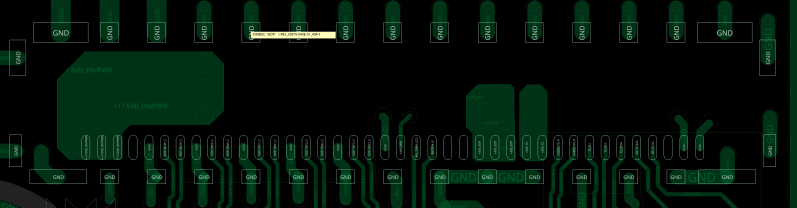
Great article! The “ramen routing” section is actually trace length matching (serpentine routing). DP uses differential signal pairs and matching the trace length within a pair is important to maintain signal integrity and lower EMI. Also common on PC motherboards (i.e PCI bus lanes).
A couple references:
https://e2e.ti.com/cfs-file/__key/CommunityServer.Discussions.Components.Files/48/0552.Texas-Instruments-DisplayPort-Design-Guide.pdf
https://www.nxp.com/docs/en/application-note/AN10798.pdf
I’ve read both of these appnotes and more. You are supposed to keep the tracks together, and also make sure that the amount of via transitions is equal on each track – this routing does neither, if you look closely. Also, the tracks travel a straight path, so it’s not even clear why you’d need to do any considerable amount of length matching here, much less in the way it was done. So, it’s just puzzling on why things were done this way, but, again, it’s fun to see that it works!
Good points. Admittedly I did not look super close because the text silkscreen was in the way. Took a look in Eagle. It is definitely curious routing, but if it works? Thanks for your in depth articles!
yeah my bad on that, should’ve made a better pic. and, glad to hear you’ve liked the articles! ^~^
All of those Adafruit products are discontinued. I just happen to have a dead 3rd-gen iPad lying around and would love to put one of these adapters on it. Does anyone have a link to a reliable seller of one of these driver boards?
I got this one to use some spare iPad3/4 LCDs: abusemark.com/store/index.php?main_page=product_info&cPath=3&products_id=47
It’s been working great for me, though it’s a bit impractical without any mounting to the panel.
They ship from Japan but it didn’t take too long to arrive for me. That store also has some different versions with DP, miniDP, microHDMI and USB-C.
I wonder if anyone has written a series this in depth but for HDMI? Oh wait, HDMI is proprietary and anyone who did write something that exposed all the secrets would probably be hit with takedowns or sued over it…
https://www.ti.com/lit/ds/symlink/sn65dsi86.pdf might be interesting for those wanting to avoid too many layers of conversion.
If you only need one reason why DisplayPort IS NOT the future, is the connector – I have the questionable honor of plugging/unplugging one of those regularly, and the executive summary is that my life would be 10000000000000000000% better if I didn’t have to do that.
really great article.
Hello!
I have a 15″ LCD panel from and old Microsoft Surface Book 2 and I want to convert it into an external HDMI display. The panel has a broken corner, so I had to replace it, but it’s fully functional.
The panel is a Philips LG model is LP150QD1-SPA1 and its resolution is 3240×2160. A search on the Internet for a suitable controller board resulted in nothing, and as I believe it a pity to waste such hi-res display, I’m thinking on alternative boards I could use.
I’ve found some eDP boards that I might use, but I believe I need something that could drive the backlight besides the LCD eDP panel itself, right? Anyway, the boards I found have a max resolution of 2560×1440, and even this one seems to be very specific (Innolux). They average on a resolution as high as 1920×1080 max.
I then came across some 4K controller boards that claim to be “agnostic” as long as the LCD panel has eDP connection. I wonder if I should buy one and give it try, since my LCD panel is only a few pixels short from the 3840×2160 4K resolution… Besides, my panel is said to be eDP 60 pins, while these boards usually manage 30 or 40 pins eDP. I believe this may not be an issue, and the 20 additional pins must be dedicated to other non-eDP standard functions, like touch and the sort.
Does anybody have any good advice?
Thanks,
Cesar