The proliferation of microcontrollers has made it easier than ever to add some smarts to a project, but sometimes there just isn’t enough space for headers on a board, or you feel a little silly soldering something that will get used to flash a program then languish inside your build. [Dima] wanted to make his boards easier to flash, and developed a PCB footprint and flashing tool pair that makes use of the mounting holes on his boards.
While some debugging tools might use a clamp or tape, [Dima] discovered that using sprung pins only on one side of the connector wedged his fixed locator pin (originally a 1 mm drill bit) into the hole removing the need for any other holding mechanism.
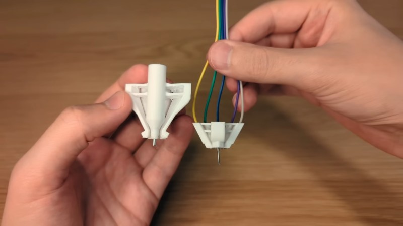
His original prototype worked so well that it took him some time to get back around to making a more reproducible design that didn’t involve fine soldering and superglue. After enlarging the contact pads and several iterations of 3D printing, he developed an interface connector that uses standard jumper wires and a steel rod to provide a sturdy and reliable connection for flashing boards with the corresponding footprint. He’s currently a little disappointed with the overall size of the connector though, and is soliciting feedback on how to make it smaller.
While [Dima]’s MCU of choice is the STM32, but this design should be applicable to any other microcontrollers using a five wire system, or you could take one off for USB. Having trouble finding the SWD points on an existing device? Try this method.
Thanks to [DjBiohazard] for the tip!


WR-WST (490107670612) has dimensions for debugging purposes and 50 mating cycles, while accepting standard ribbon cable or strips of ready-made Mini-PV patch cable. Probably worth considering under the constraints set forth here.
It’s a kind of low force press-fit wire-to-board solution and the “SKEDD” contacts used press against via barrels without a static force holding the connector in place.
Those are absolutely great. Have used them on a number of boards. The fun this is, Wurth has two footprint options for the connector. One with a click, that sits a little more tight, mostly used for a more permanent fix, for example board to board connections in a system. The other footprint is what i have used a lot for debugging. It has a less tight fit and can be disconnected more easily.
I second SKEDD. It is the best thing to debug interfaces. You can have minimal pads since the contact is made in the through-hole. You can have it even in a PCB panel where it appears just as holes. Also you can place other connectors on top, like a 2x Wago 243-211 (KNX), and normally you just have the KNX connector but as you remove you can connect 4 pins with SKEDD (they are just the same width)
JST SCN connector can be another option for regular pin holes. And it can be used as losses wires.
Neat, I hadn’t seen these before. 50 mating cycles seems quite low for a debug connector. Depending on how many devices I’m juggling, I could see doing 50 cycles in a week.
It’s fünfzig in germany, in regular countries you can use it much more :) The through hole plating will probably the limitation, so they can’t rate it too much as the PCBs can have different qualities. I’ve used mine over 50 times in the first day alone :D
I think his first attempt with the pogo pins is the best version. It’s small so doesn’t need as large a footprint or exclusion zone as the latest version. Yes, there’s soldering and superglue, but if someone is building a board and wants to use this to program it, chances are they’re accustomed to soldering.
Yeah if I was going to reproduce this, I would probably stick with the pogo pins and rather than using 3D prints, I would use a small round PCB to solder the pogo pins with additional holes for the 1mm rod and the bolt. If the PCB wouldn’t hold everything in alignment well enough then I might add a 3D print and glue it to the PCB to give it more thickness where needed.
“His original prototype worked so well that it took him some time to get back around to making a more reproducible design that didn’t involve fine soldering and superglue.”
i love that. that’s one of my favorite patterns in prototyping. when you discover to your surprise, “actually i’m done!”
Lol yeah and the surprise with it
Steel pins, at this scale that sounds like piano wire. The most assertive to-the-point probe-point you can probe with, or if you want to hold it long to enough flash a chip. Better, just rig a third hand device to hold the probe anywhere there is a lead or pad.
So, I’m not a hardware designer by far. But 3 questions.
He wants springiness to ensure a good contact. The pogo pins are perfect for that. Baring that, why not… Tiny springs? Why 3d print a spring for the mount when you can use a coiled conductive material to start with?
Why is the locating pin so long? If this is installed in a device, the locating pin seems like it would get in the way. Honestly, maybe double the depth of of the PCB should be plenty for the angle locking to work. And on that note …
Why is the central carrier bolt not the connecting mechanism? Need to reflash something? Unscrew to programming screw, screw this in. Locator gets it at the right angle and screw secures it down. This seems ideal for units already mounted and installed.
Option 2 for me would be similar to the twist lock pins for CPU fans. When you push it down, it expands and locks the device in, and you rotate to lock the pin. Reverse to disconnect. This would be ideal for units that have yet to be mounted due to the excess exterior spaced behind the unit.
Microchip has a similar method to flash & debug:
https://www.tag-connect.com
We use these for debugging SMT32 (SWD) and programming eeprom chips at the company I work with. Very convenient, love them, albeit they are quite pricey.
Yeah, price is a bit high, but damn do they work well.
I wanted to implement that in one of my recent projects, it looked super nice and compact. Then I looked at the price. FIFTY bucks? For fifty bucks I’d rather hold dupont wires in tension with my hand and type openocd commands with the other (which is exactly what I ended up doing)
that’s for a kit, but you can get the bits off digikey, we use them here in the lab
This is tag connect not Microchip. And they have a patent on a spring loaded debug connector, which is why they have a monopoly on the connecter and can charge a fortune for them.
Yes, he already shows the tag-connect connectors @02:04 in his video.
At some point, we got into ESPs. A jumper is enough to activate OTA for Debugging. The actual debugging is done on a wired model – never experiment on workhorses.
But in principle, spring terminals are a good solution. After all, the USB heads for the Raspberry Pi Zero, for example, do exactly that (only on conductors).
This reminder me of the no longer available eurocircuits ec-test-mate; https://www.eurocircuits.com/test/
I always use tag connect footprint and cables, it’s small enough.
Did this in the past: https://github.com/X-Ryl669/SOICconnect
It’s using 3$ SOICbite plugs and a 3D print for the connector. On the PCB, it takes almost no space. You got springs in the bite stuff and a alignment tool on the PCB’s footprint so it’s not possible to connect wrongly. If it bites, it works.
Tag-connect anyone??
Please no, it’s awful and stupidly expensive ^^
SKEDD or SOICbite are much better from a user experience point of view and dirty cheap
On one hand too expensive. On the other, I prefer not supporting patents.
Another classic is the ‘pressure loss sensor’ in cars. The simplest solution is the Indirect TPMS, which uses the rotational speed of the tyres and the vehicle’s speed data to evaluate whether the tyre pressure, and therefore the tyre size, has changed.
It works more slowly than a direct measurement but is sufficiently reliable and works with every tyre. And as is often said with technical systems: one less sensor is one less source of error.
seems to be on the wrong article :)
but that’s a neat approach! i have always thought the idea of having tiny battery-powered sensors in each tire is nuts. how do they measure vehicle speed separately from tire rotation though? seems like the easiest option would be to measure rotation of all the tires separately, or to measure slip at the differentials??
I like the original, but let’s skip the plastic. Pogos through a PCB for support and electrical connection. The pogos are simply pushed through the PCB and soldered in place. The PCB can then shift the signals to a convenient point where an optional connector can carry it away. A second PCB can even be added if additional support is needed.