Some time ago, while designing the PCB for the Sony Vaio replacement motherboard, I went on a quest to find a perfect 5 V boost regulator. Requirements are simple – output 5 V at about 2A , with input ranging from 3 V to 5 V, and when the input is 5 V, go into “100% duty” (“pass-through”/”bypass”) mode where the output is directly powered from the input, saving me from any conversion inefficiencies for USB port power when a charger is connected. Plus, a single EN pin, no digital configuration, small footprint, no BGA, no unsolicited services or offers – what more could one ask for.
As usual, I go to an online shop, set the parameters: single channel, all topologies that say “boost” in the name, output range, sort by price, download datasheets one by one and see what kind of nice chips I can find. Eventually, I found the holy grail chip for me, the MIC2876, originally from Micrel, now made by Microchip.
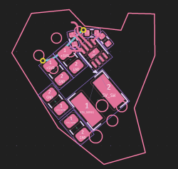
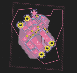
MIC2876 is a 5 V regulator with the exact features I describe above – to a T! It also comes with cool features, like a PG “Power good” output, bidirectional load disconnect (voltage applied to output won’t leak into input), EMI reduction and efficiency modes, and it’s decently cheap. I put it on the Sony Vaio board among five other regulators, ordered the board, assembled it, powered it up, and applied a positive logic level onto the regulator’s EN pin.
Immediately, I saw the regulator producing 3 V output accompanied by loud buzzing noise – as opposed to producing 5 V output without any audible noise. Here’s how the regulator ended up failing, how exactly I screwed up the design, and how I’m creating a mod board to fix it – so that the boards I meticulously assembled, don’t go to waste.
Some Background… Noise
This regulator is one angry chip – with a 2 MHz switching speed, it’s relatively high as far as regulators go. More common is to see 1 MHz and below. Higher switching speed means it can use a smaller inductor, which is great for routability. It also might not handle some layout or component mistakes that a lower-frequency regulator might do.
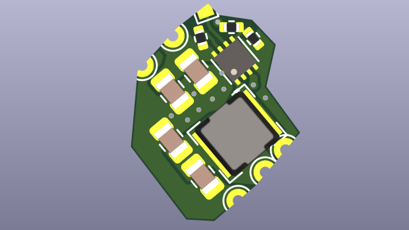
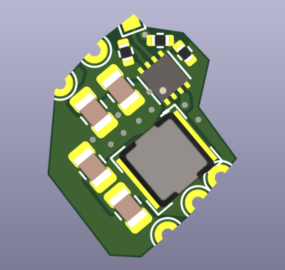
Still, I made a number of good choices. With boost regulators, remember – you have to pick an inductor according to the input current, not output current; recalculate accordingly, and check the efficiency graphs. That, I achieved – while I was limited by the size of the inductor I could fit onto the board, I did find a 3.8 A inductor that let me achieve a little under 2 A output. Iin theory – good enough. All places where 5 V could go on the board are current-limited, and there are just two USB ports I need to power, so even 1.5 A of 5 V output is plenty. I also picked proper footprints for both inductors and capacitors – it can be tricky to find 22 uF 10 V capacitors in 0603, but it’s a breeze if you pick 0805. A regulator can fail if you don’t provide it with the kind of capacitance that the datasheet asks for, but I put two footprints on both input and output, and it let me experiment with output caps.
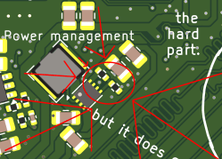
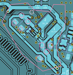
On the other hand, you might have already noticed at least one problem if you’ve read the layout article thoroughly. For one, see that feedback divider? It’s supposed to be connected after the capacitors, measuring the output – not directly between the inductor and the capacitors, which is a point where a lot of current flows back and forth. I’m not sure how I didn’t catch myself doing this, given that I thoroughly described in an article in the same timeframe that I was routing this board; it’s the kind of mistake you can’t help but write off to general human fallibility. There are a good few problems, though – I should have reconsidered this layout severely before ordering.
Example Layout As Checklist Item
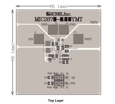
A contributing factor, I’m sure, is that the datasheet doesn’t have a layout example – you only have the evaluation board documentation to go off of, and I didn’t get that far. It’s not always that the datasheet recommendation will be reasonable, or look reasonable. For instance, in the last article, where I reviewed switching regulator layouts, I’ve shown the TI’s puzzling proposed layout for a buck regulator chip of theirs – with intentions hard to decypher both for me and for fellow hackers in the comment section.
However, it helps way more often than it might puzzle you, and if you never even see the layout example because you have to hunt down extra documents for it, you might not notice fundamental differences, just like I did not notice them. The bottom line is I should have noticed the missing layout example and hunted down the evaluation board datasheet.
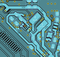
Comparing mine with the example layout, you might notice another problem. My ground routing differs a fair bit, and it sure seems that my routing is inferior – my ground is more isolated islands, with a fair bit of ground return current forced to go through vias, and the example layout has a fairly straightforward ground path, no underside layers strictly required. What’s more – you might notice ground return current flowing between output capacitors and the regulator center pad, which will go by the pin 4 – AGND. AGND is specifically a pin supposed to stay away from the switching loop pins, and I do remember noticing this at some point, thinking I should revisit the layout and see if I have fulfilled this obligation. It stayed as a low-level mental TODO in my brain, one that I never actually revisited.
One last thing is placing components under the regulator. I can’t quite afford to free up the under-regulator space on the opposite layer of the board – the board is tightly packed by necessity. My defense is that this is a 4-layer board, with two inner layers dedicated to ground, but I’m not sure whether that negates the concerns of the engineers who wrote this recommendation. This is the only thing I’m leaving in when it comes to v2 board design – otherwise, let’s take a look!

Out of interest and wanting to finally get to the bringup, I re-wired the FB connection using magnet wire, and even added a more direct GND connection for the output capacitors along the way. The regulator’s behaviour didn’t change one bit, however. Either the GND layout is seriously critical (likely), or the chip got damaged after being booted up with a miswired feedback network; whichever option it is, looks like things won’t be as quick as that. In general, I spent four-five hours on this particular issue, slowly realizing that it’s screwed up beyond fixing.
No matter – let’s just design a mod board that works around all of my mistakes. This helps me bring up the v1 PCB fully – wouldn’t want to have $300 worth of components and days of assembly going to waste. Also, after just a few modifications, we will have a cool switching regulator breakout that we can all use as a building block!
Quick, Simple, Powerful
To make a modification like this, I start by marking an outline of the mod on one of the User layers, then open the file in a text editor, Ctrl-F for the User layer name I used, copy all the lines and circles – and paste them into a footprint .kicad_mod file that’s also open in a text editor. There are a few caveats – first one, the User.Eco2 layer in KiCad UI is called Eco2.User in the actual file. Then, as you copy-paste graphics you’ve drawn, you will also want to replace all “gr_” with “fp_”. Remember to close your kicad_mod while pasting contents into it in the text editor – otherwise, it can be overwritten by accident. Finally, open your .kicad_mod in the footprint viewer, box-select your new lines, and move them so that the (0,0) center point is somewhere near the outline, because it’s going to be a bother to handle this footprint otherwise.


 Then, open a new PCB project, copy-paste the 5 V boost schematic block into the schematic, open the footprint association view and bring over any footprints missing, sync the PCB file, then duplicate the evaluation board layout. Thanks to this workflow, I quickly created a 5 V boost mod board I can solder on top of the board I currently have. This board is about to be ordered, with proper layout, and I’ll soon be soldering it onto the motherboard then testing it – expect an update in the comment section.
There are five (or, four and a half) other switching regulators on the same board, and, as I’m bringing them up and testing them, I’ll write one more article where I will be sharing lessons, whatever they turn out, showing you examples of how to pick parts for a switching regulator, plus, most certainly, demonstrating a couple more more little ways you might get things wrong and how to avoid them. So, till next time!


I’ve done a little bit of design with switching regulators, but I had the luxuries of slightly slower speeds and enough room to follow the (readily available) manufacturer’s recommended layout fairly closely. Kudos to you for finding a viable workaround to a problem which was in part caused by poor availability of relevant documentation.
Kudos as well for how far you’ve come, both as a writer and as a designer, since you joined Hackaday. It’s a pleasure to read your articles.
You can find 22uF in 0402 (that’s what I source usually). I think you’re overengineering your problem. The layout is/might be important, but what you are observing isn’t a layout issue, but a routing issue and probably a mounting issue, IMHO.
There’s no need for 45° rotated components and 4 layers for such a regulator. A plain old 2D with 0° and 90° orientation and 2 planes would have worked. If the regulator output 3V and make audible noise, it means that it’s oscillating at a much lower frequency that it should and this is not due to bad feedback but a current consumption that’s too high further down the line. A bad feedback will give a noisy output but doesn’t prevent the regulator to oscillate. So if I were you, I’d isolate your regulator (if you can) from the sink underneath, and it’ll likely boot up as expected. Then I’d look as the powergood line to see if I can disconnect it from the next circuit (but leaving the Vout connected) to check if I have a short. If it fails, the next circuit is the culprit, if it doesn’t that it’s its boot current that’s too high (meaning likely a bad configuration for the powergood voltage threshold and/or a bad capacitance on this line).
I might be wrong, but it looks like your VIN_5VREG net isn’t connected to the VIN net (under the inductor) (on the “layout as manufactured” diagram). It should be directly connected with a large copper plane.
Also, on the proposed layout, they are filtering the bottom resistor of the feedback divider with a RC which you didn’t do on your design (but you can change by desoldering the bottom resistor and soldering magnet wire to a R/RC circuit). I don’t know why it would be required, maybe to start oscillating faster, since on start up, the FB pin will read 0V (while the capacitor charges) instead of the expected divided voltage and this might force the regulator to boost for longer.
VIN_5VREG and VIN are two different nets which are created by two different ideal diode chips. The proposed RC circuit is unpopulated in practice on the devboard, and isn’t present on the example schematic – that, and I haven’t even gotten to the point where thinking about adding RC circuit would be worthwhile.
4 layers are because the board itself needs them, and the 45 degree rotation is because of other tracks and components around the regulator – this regulator doesn’t exist in a vacuum =D As for current consumption, the regulator was doing that both without load and with load. Also, I checked for shorts first and foremost, and then all throughout, same went for bad capacitance exploration – as I describe.
Small caps like that collapse under bias. The best you can get with 0402 22 uF is 6.3V max and at 5V, it’s lost 90% of its capacitance.
Those guys are for decoupling like a sub-1V rail, not ~5V-ish.
There are 10V 22uF in 0402 also (look here: https://eu.mouser.com/datasheet/2/281/1/GRM158R61A226ME15_01A-1984486.pdf ). They don’t “collapse” at the rated voltage, as you said, look at page 11 for a graph, it’s pretty flat in the [0-rated voltage] range. Even in the cheap 6.3V for kyocera one, the loss is < 12% at 1.5x the rated voltage (so around 10V), which is very manageable. Even if you are paranoid, you can use the 0603 footprint with 47uF so you have plenty of margin.
No, those are example curves, not the actual curve! God, I hate manufacturers for doing that, I’ve been bitten by that before.
The actual curve for that guy is here:
https://www.murata.com/en-us/products/productdetail?partno=GRM158R61A226ME15%23
and as you can see at 5V it’s down -82.2%, as in its actual capacitance is ~4 uF.
It’s the same for the Kyocera 6.3V guys (https://ele.kyocera.com/en/product/capacitor/mlcc/kgm/kgm05cr50j226mh/) , which you can see in the Characteristic Data linked off there.
No one reports data above the actual voltage rating, that would be psychotic.
Nice catch.
On the other hand why do you create a new patch board just to re-route that single trace? Instead of tombstoning that single resistor, soldering a small wire onto it then the other end to the output, then with some uv resin fixate it in place. 5 minute job, instead of the multiple hours + patch board + waiting + etc.
(Not just the feedback line, but the GND too, drill the vias out, solder a wire into it, scrape the soldermask, solder it across to the other gnd plane.)
yeah see drilling a 4 layer board’s vias is where I opt into creating a patch board =D I have other things to bringup on it!
I’ve already done that, 0.1mm magnet wire rewiring the FB upper leg, didn’t change much! it’s not just a trace reroute, it’s also realizing I have created a board where some of the current flows by AGND, and ground availability is subpar – at that point, rerouting and creating a patch board started to look way more promising.
$300 sunk into a prototype confuses me. this reminds me of a discussion on an article about ch32v003 or something, a ridiculously cheap microcontroller with the caveat that it’s only available surface mount and from relatively non-reputable vendors. i said, unless you’re building a zillion units, why do you care about the price so much that you’ll accept that difficulty? and it seems like several people replied to say that i was overestimating both the difficulty and the expense of prototype quantities of populated custom boards with the ch32v003. which seems plausible and i dream of the opportunity to test its truth. :)
i’m mostly ignorant about all of this so i have a question: since it was a prototype, why did you order $300 worth of it? i’m still struggling to understand this intermediate scale of development, in between one-offs (like my workbench) and mass production. was it possible to buy a single unit for $10 but you made (what in hindsight looks like) a mistake, or is the cost for low-count prototyping that unfavorable in practice?
thanks!
AIUI, Arya was building 5 different Vreg prototypes on one PCB build order.
Maybe the $300 was the total cost of that run.
In short, I’m comfortable making a bet on this project working out for me, which is why I’m investing into its first stages so much. ~$300 is a total investment into the project so far, and it’s because 1) the project is complex, 2) the ICs are semi expensive, and 3) I’m also planning for future boards as I go. This batch is 2pcs, but I’ve ordered quite a few support components in 12pcs instead, making the next batch sourcing way easier on me. $300 adds up quick – there’s a Zero W 2 on every board, a sprinkle of ICs that are a dollar-two each if not more, add the more expensive passives like inductors, a myriad of cheap passives (a hundred caps and resistors on every board!), the fun connectors that the original board used, shipping costs for both two separate parts orders and the boards, and undoubtedly some things I forgot. I used quite a few price saving tactics, but cost-wise, such projects can still have quite a steep financial barrier of entry! Single unit for $10 – no way, sadly, this is an integrated enough board that I can’t quite afford using any pre-made modules, it’s one of its kind, and given how many different subsystems it requires, I don’t see how it could ever be made for $10.
As for ICs like CH32V003 – it’s fun, it’s an alternative to Western chips in quite a few different ways, it’s a new ecosystem to explore, indeed, it also opens up the “make 100pcs of something” possibility way more than Western chips do, and the difficulty isn’t really there either. As for “non-reputable”, this only stands for a certain standard of reputability, which not everyone really cares about. Oh, don’t forget, automated PCB assembly from China is pretty cheap and easy to use compared to Western offerings, so Eastern chips are also advantageous in that they don’t need to be imported into China, driving up cost for no good reason. Also, speaking about SMD, it’s not more difficult than THT – just like Linux vs Windows, it largely matters what you have more experience with.
thank you! i think i understand now. i didn’t properly understand the scale of the board, even though that was really the point of the article. so it’s only expensive because you’re prototyping a lot of things at once, and many of the things are fairly expensive.
fwiw i think it’s ableist to say surface mount is as easy as through hole :) (my hands shake)
I once worked with a guy who would spend months reviewing his design, double checking this, triple checking that, and then checking again anyway.
My philosophy was to crack on and prototype. Used to drive the boss nuts. Do the design, lay out the board, and check it (I’m not so stupid as to not even check it!). Send out for a prototype. Hook in to project #2 while waiting for the return. Once back, test: likelihood of poor performance – reasonable. But sometimes it worked first go. In many cases the total time taken (not man hours) for the one project was the same, but I was able to interleave a second project.
Short version: Back then I was getting about $50 an hour. In a commercial setting, $300 would equate to about 6 hours, or less than a day. Hence: PROTOTYPE OFTEN – it’s truly ends up being a damn side cheaper!
PS: The same applies to 3D printing. Scratch up your design pronto, send to printer, and work on revision n+1 while waiting. Loop again.
Fire up the oscilloscope my good man, let’s have a look at what is actually going on with the errant regulator.
Perhaps I’m missing something from your text editor trick, but you can copy-paste shapes directly from the board editor to the footprint editor. I don’t see a reason to go through the text editor.
oh if that’s the case, that’s pretty cool! I think I tried that recently and it didn’t work out, so I went the old way. It would make things even quicker on me – I’ll retry next time!
Arya:
“it can be tricky to find 22 uF 10 V capacitors in 0603, but it’s a breeze if you pick 0805.”
Well, I just got bit by this, so I’d figure I’ll pass it on!
No, it is not a breeze to find 22 uF capacitors in 0805 that are still 22 uF at 5V!
Literally all of Murata’s 22 uF caps are under 10 uF effective at a DC bias of 5V. Some of them are like, 5 uF or less! The best you can do is around 12-13 uF at a DC bias of 5V, and that’s a 47 uF cap (at 6.3V rating, there’s a 100 uF cap which is 20 uF at 5V, but that voltage rating is too tight for me).
Yes, let me be clear: you may get more capacitance from a 10 uF cap @ 5V than a 22 uF cap @ 5V. You really have to be careful with ceramic caps.
There may be some from other manufacturers that have less of a falloff, but Murata’s SimSurfing tool has an “Advanced Search” which allows you to specify “capacitance at a DC bias” and so you can very quickly see what they really are.
This is one of the big advantages of electrolytics: they have a flat capacitance vs DC bias, because they’re not piezoelectric.
Ceramic? As in those disc capacitors?
But you are mentioning 22 ufd. not pfd. And SMD as opposed to THT.
I’m confused, and not criticizing what you wrote, it’s just that DC bias part.
Most chip capacitors you see are ceramic. MLCCs stands for multilayer ceramic capacitor. And yes, MLCCs are piezoelectric.
Oh, and I have my suspicion that this is exactly the problem Arya found.
https://www.reddit.com/r/embedded/comments/1cs2c5l/todays_reminder_that_mlccs_lose_capacitance_with/
I thought about this in the multiple-hours debugging session, and, no, sadly, that was not the issue! Datasheet says a single 22uF is necessary, iirc mine were 6.3V or 10V. I have two cap footprints, first I populated one 22uF, then I populated two 22uFs in parallel – made no difference whatsoever. As a rule, I make sure I can add more caps than datasheet recommends, and over-rate them accordingly.
22 uF 0603s are extremely low in capacitance with bias – like, 4 uF at 5V. So even dropping 2 might not make a difference.
In fact once you get past about 2V, you’re often better off putting two in series than two in parallel. Lets you use cheaper caps, too, because the cap change over voltage is absolute, not relative to the max rating – it’s just falling like 1/V (because… that’s what the electrode distance is doing). So putting 5 22 uF caps in parallel at 10V is actually slightly worse (around 15 uF total!) than 5 of them in series (around 16 total).
Obviously it makes the ESR worse so it’s not a total trade, but ceramic caps have such absurdly low ESR it often doesn’t matter.
SimSurfing actually lets you plot multiple caps overtop of each other, so you can see this directly. Just grab a bunch of caps all with the same size and nominal rating (regardless of rating), plot capacitance vs bias, and they’ll all overlay each other right on top. It’s just electric field stress.
ohhhh that tool sounds indispensable, I should check it out! I try and look out for Murata caps anyway, so it could be a nice reference for learning more while at it.
Thanks for the advice, and the “advanced search” tip!
The best “fix” is to ommit the switching stuff and go for a clean, linear design.
Or use an optical way for conversion. If it’s in the mA range, it might be possible to use a photodiode or solarcell and a light source.
A buffer capacitor can be used on both sides to smooth out the power.
“The best “fix” is to ommit the switching stuff and go for a clean, linear design.”
please upload your linear design for a boost regulator, tons of us would love to see it
The way this reads, it makes absolutely zero sense for the requirements I outline in the article – unless you can elaborate a fair bit on what exactly you mean and how it’d help me.
A good proposal for a fix is one that actually applies to the application in question and unless you are sitting on some miraculous Linear design for powering 5V USB devices from a 3.3V rail. This is a BAD proposal.