
Today’s PCB design review is a board is from [Wificable]. iI’s a novel dual-SSD laptop adapter board! See, CPUs and chipsets often let you split wide PCIe links into multiple smaller width links. This board relies on a specific laptop with a specific CPU series, and a BIOS mod, to put two M.2 NVMe SSDs into a single SSD slot of a specific series’ laptop.
This board has two crucial factors – mechanical compatibility, and electrical function. Looking into mechanics, it’s a 0.8 mm thick PCB that plugs into a M.2 socket, and it has sockets for two SSDs on it – plenty of bending going on. For electronics, it has a PCIe REFCLK clock buffer, that [Wificable] found on Mouser – a must have for PCIe bifurcation, and a must-work for this board’s core! Apart from that, this is a 4-layer board, it basically has to be for diffpairs to work first-try.
Of course, the clock buffer chip is the main active component and the focus of the board, most likely mistakes will happen there – let’s look at the chip first.
All Eyes On Chip
The schematic is from a server board schematic – which is wonderful! Datasheet schematics are not always as complete or as succinct as you’d like them to be, and it’s super helpful to have a known-working schematic designed by a third party, that is production-grade and well-tested for 24/7 operation. We used that for our M.2 card design,
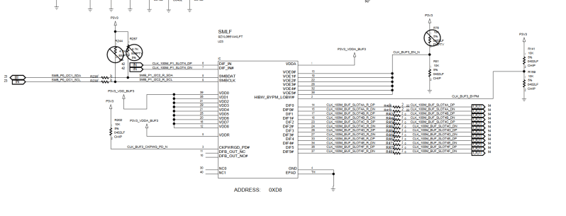
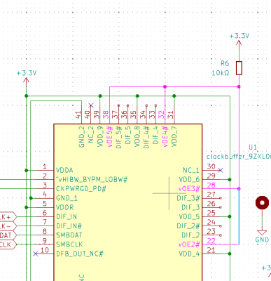
Of course, the symbol had to be redrawn for KiCad, and [Wificable] also rearranged the symbol corresponding to the physical pinout, as opposed to arranging them logically, like many KiCad symbols do. This is mostly a matter of preference and either way is fair – I switch between either of the two, depending on the situation. One note, though – when copying a schematic, I highly recommend you use the same pin arrangement as that schematic, it’s just really helpful to avoid mistakes.
In this case, I’d argue the logical arrangement is also cleaner, and that’s what I’d personally go for. However, design reviews are about function way more than aesthetics, and the chip’s wiring looked fine!
In my view, policing aesthetics is generally a no-go for PCB design – most you can do is suggestions. The line between aesthetic problems and practical problems is often blurry, let’s say, when the problem is about track routing, connector layout, making the schematic easy to check at a glance, or a good few other things. When in doubt, think about the best effort-to-payoff ratio for the person receiving the review.
Layout-wise, things are also fine – but they could be a little finer. The decoupling capacitors do need vias on their GND pads – easy to add, and a big benefit as far as power delivery goes. There are other areas where vias are called for! That, or having vias arranged a little differently, at the very least. Let’s take a look!
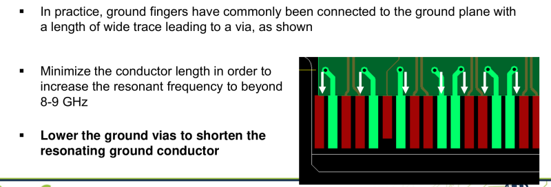
Well-Grounded
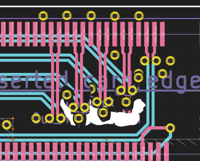
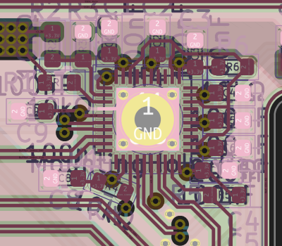
There are quite a few ground-related changes I’d recommend here specifically, given that it’s a high-speed design. I’ve been reading a fair few “how to treat ground fills better” documents, and they discuss about a row of signals with vias, ground unable to get between them. The recommended way is to arrange the vias diagonally, instead, letting some of the ground polygon fill between the gaps and freeing up space for GND vias – and that’s what we can do here, too.
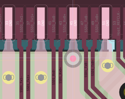
Do Not Bend
For dessert, we look at mechanics more closely. One thing that springs out to me – this is a 0.8 mm board inserted into a M.2 socket. The cutout in the middle is a liability. Some sort of cutout is necessary to accomodate plastic features of the laptop, but having a wide center-to-edge slot is a recipe for PCB bends. In this case, the edge-to-center slot can become a shorter one, mechanically connected on the edge again, just needs a little bit more measurement.
So far, the boards have been produced, thanks to Aisler’s new 0.8 mm four-layer process. They’ve been partially tested: [Wificable] didn’t get the chip yet, but has already successfully done the BIOS mod, and tested the bifurcation using magnet wire to switch between REFCLKs. Whenever [Wificable] finds time to finish testing, we will hear from her about how well the chip functions!
As usual, if you would like a design review for your board, submit a tip to us with [design review] in the title, linking to your board files. KiCad design files strongly preferred, both repository-stored files (GitHub/GitLab/etc) and shady Google Drive/Dropbox/etc .zip links are accepted.


Is there any mobo that allow m2 x4 biffurcation to 2x2x ?
Ive been thinking of making something to put two 2230 drives into a 2280 slot, and then never got around to it. This is going to save me a ton of time. I just have to change the board layout.
It was a feature of Intel 7th (possibly 8th and 9th+?) generation hybrid Optane drives.
There was an Optane memory cache and an SSD on a single M.2.
The maximum theoretical bandwidth was obviously lower than a regular SSD. However since Optane excells at random access there was noticeably reduced latency when using the OS.
It is very sad optane went away, with PCIe 5.0 it could have been fast enough for regular users, while providing the reduced latencies that make a computer feel more responsive.
Since it relied on x2/x2 bifurcation the drives only came in select laptops.
How do people feel about via-in-pad to minimize the inductive loop area? (How do people feel about increasing the solderpaste cutout area to provide more solderpaste for filling in a via-in-pad so there’s still enough for the leg fillet?)
In my experience, via-in-pad can be used without issue if you follow TI’s PowerPad guidelines https://www.ti.com/lit/an/slma002h/slma002h.pdf . I’m sure you could get good results without following them, but I’d rather not spend the time and money testing other options when TI have already done the testing.
These work fine even if your PCB manufacturer doesn’t officially support via-in-pad.
@Dennis C Are you only talking about heat-spreading vias in thermal pads that are effectively ground-pour? I didn’t see anything in there about signal vias, except for a sort of offhand comment that it would be OK if they interrupted the thermal pad.
Even for heat-spreading vias, I’m not sure I saw a recommendation beyond “use the enhanced TI PowerPad(TM) package” and “defer to the datasheet for a particular device”, but it did look like the example land patterns all used 0.3mm vias on a 1.5mm pitch. And to answer @smellsofbikes they suggested blocking those vias with solder mask, and warned against using too much solder. (It looked like you needed at least 30% fill for good heat spreading; they suggested aiming for 50% but trusting your assembler to override that, because the assembler would know what was too much in practice for their own process.)
Plugged vias are not that expensive anymore, JLCPCB offers them as standard for 4 layers. That mostly resolves any via-in-pad issues for larger pads.
To put a via in e.g. 0402 capacitor pad, you’ll still need plated-over vias, which costs slightly more.
They offer plugged and plated over vias for free for 6+ layer boards, which also costs only 2USD for boards less than 52mm×52mm as a special offer.
It really depends on the project. For a lab only design where you can hand-tune and rework all the soldering, you can try much more wild stuff.
If you however plan to do some production runs, plugged and capped vias are basically the only way to get reliable solder quality. Another problem you might run into is tombstone effects with vias in pads of passive components. With much more copper and thermal mass on one side of the component, the tendency to get tombstones increases a lot. But again, this depends a lot on the reflow process and you will get different results on a vapor-phase or inline reflow with lots of different temperature zones, compared to a simpler reflow setup.
Trying to adjust the amount of paste to fill the via again is a “hack” that might work for one-off lab designs, but probably never the right way for a production board. If you actually need via in pad at all, or if the design works just as good with traditoinal technique is something you can only really evaluate if you do both designs and compare/measure them…
Would have liked to see more Guard VIAs when switching copper layers, but looks ok enough to likely work.
Is that just based on the pictures right under the “WELL-GROUNDED” section header, or do you see the actual design files, or at least a full set of gerbers?
Where would one look to learn more about this x2-bifurcating BIOS mod?
I happen to have acquired an Optane H10 drive, which has 16GB of Optane and 256GB of QLC, with each getting its own x2 allocation on the m.2 connector. Apparently many Optane-compatible chipsets exposed this x2 bifurcation option in their BIOS, and some devices like the Odroid H4 have specific BIOS versions you can flash to enable different PCIe topologies.
However, it’s been difficult to find out how this sort of BIOS tweaking might work in practice…
There is a guide on Level1Techs that walks through using AMIBCP to track down and enable hidden settings in the pre-existing BIOS, and so I suppose it is possible that the answer is simply that if your BIOS does not implement x2 configurations (hidden or not) then it’s just not possible – hence the requirement for a specific CPU and laptop with the board mentioned here.
https://winraid.level1techs.com/t/guide-how-to-bifurcate-a-pci-e-slot/32279
Be aware that AMIBCP tends to not work anymore on more recent BIOSses, it either crashes when you try to save or it produces a corrupted image. AMI seems to have deprecated it.
But you can get very similar results with AMISCE. Sometimes you have to enable options regarding HII or config write protection before it works though.
About the bifurcation: some manufacturers have an automatic bifurcation implemented, some code that tests what is plugged in and then assigns the lanes accordingly. With one of these you don’t need any BIOS mod or option. If your system does not have that, then you need a visible or hidden option to enable with AMISCE (or AMIBCP). And for both to work it must be an AMI-based BIOS of course.
Unfortunately no alternative way than getting hardware and trying it out.
2×2 is tough as the chipset needs to support it as well as the UEFI setup.
I have been watching and marinating on the H10 /20 Optane drives as I would love to use them as mirrored disks for proxmox.
In my pile of kicad project ideas is a low profie x4 pcie card with a pericom pcie switch that feeds two m.2 slots with each ssd controller getting a lane. It would not be the fastest thing, but it would still give me 4 ssds that would work great for zfs mirroring.
I won’t be happy until I can furcate an x16 slot into x1x1x1x1x1x1x1x1x1x1x1x1x1x1x1x1, who can make it happen? :D
What I wanted to do is find a PCIe bridge chip that takes in say, 4xPCIe-5 lanes, and breaks it out to two sets of 4xPCIe-4 lanes.. No bifurcation mods needed, and you still get the double SSD goodness, just 1 gen behind.
The PM50028B1-FEI is exactly what you need. The ‘outputs’ are also PCIe-5 but I have never seen an asymmetric switch with different gens on one device.
How schematics look is not just a matter of preference.
Schematics must be READABLE BY HUMANS. This is paramount and should not be negotiable. It is exactly like computer program source code.
Kikad will have no problem matching the connections and components in the schematic to the board layout, no matter how clean, dirty, or convoluted the schematic diagram looks.
Schematic diagrams, like source code are generally subject to upgrades and improvements; they should not be treated as a “write once” language.
Of course, there is also a limit to how perfect a circuit diagram, or computer source code should look; at some point you must stop “improving” things that are “good enough”.
Great minds think alike. Beat me to it! Excellent job!