
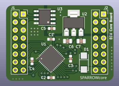
I enjoy seeing modules that can make designing other devices easier, and when I did a call for design reviews, [enp6s0] has submitted one such board to us. It’s a module called TinySparrow (GitHub), that helps you build your own vehicle ECUs and any other CAN-enabled things. With a microcontroller, plenty of GPIOs, a linear regulator and a CAN transceiver already onboard, this board has more than enough kick for anyone in hobbyist-range automotive space – and it’s surprisingly tiny!
You could build a lot of things around this module – a CAN bus analyzer or sniffer, a custom peripheral for car dashes, or even a full-blown ECU. You can even design any hardware for a robot or a piece of industrial technology that uses CAN for its backbone – we’ve all seen a few of those! It’s a great board, but it uses six layers. We’ll see if we can do something about that here.
Modules like TinySparrow will make your PCBs cheaper while ordering, too! Thanks to the carefully routed microcontroller and the CAN transmitter, whatever board you design around this chip definitely wouldn’t need six layers like this one does – and, unlike designing your own board, you can use someone’s well-tested and tailored libraries and reference circuits!
With TinySparrow, you save a lot of time, effort and money whenever you want to design a car or industrial accessory. After looking at the board files, my proposal for helping today’s board is – like last time – to make its production cheaper, so that more people can get this board into their hands if the creator ever does try and manufacture it. I also have some tips to make future improvements on this design easier, and make it more friendly for its userbase.
More Layers Not Always Better
Every single pin of the microcontroller is broken out – this matters a lot for such a module. It’s seriouslty annoying when you try to squeeze the most out of the onboard MCU, only to find out that the GPIOs broken out don’t expose one of the critical pins you need. I value such module designs a ton and I think people should be aware of their existence, which is why I’ve just spent time highlighting its strengths.
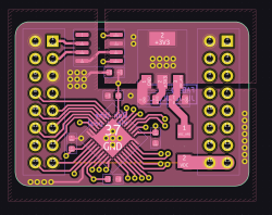
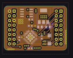
So about those layers. On one hand, this is justifiable for how tiny this design is. Three of these layers contain traces, two are uninterrupted ground fills, and another layer is 3.3 V. This is wonderful for signal integrity, and perhaps this board could really use an extra SI kick. Still, today, I would like to show you how to free up two of the layers, however – in part in case the author struggled to fit things on 4 layers, and in part to show how it’s done.
Six-layer layouts give you superiour signal integrity and a lot of space to route your traces. Often, six-layer boards are nigh unavoidable, like when doing high-speed USB-C altmodes with certain kinds of connectors. However, if these same features could be smooshed down onto four layers, it would be significantly cheaper both for the PCB and assembly.
So let’s get rid of two layers. As you can see, the layers are kinda full, so, some traces would need to be moved. For that, let’s look into the trace layout on this board. The board looks like it exceeds four-layer routing space provisions by a fair bit, but I can show you how it’s not the case!
Tweak The Defaults
For a start, let’s talk about default parameters, something that ends up limiting this board’s design. This board uses all default KiCad parameters – track widths, clearances, via diameters, and zone values. They are conservative, which is helpful for i.e. etching your own boards, but you lose that benefit if you just order the board, something inevitable at six layers. Let’s go through the distances on this board and see which values we can use while still being totally safe for manufacturing. After we dial the values down, we will have a lot more freedom for rerouting this board!
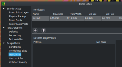
Track width is at 0.25 mm by default, but it can go as low as 6 mil on any self-respecting fab. Same for the 0.2 mm clearances – they can go to 6 mil too. On 4-layer and 6-layer boards, you can go down to 0.09 mm / 0.09 mm, which especially helps with diffpair layout, but also helps you pull track bundles from point to point.
Vias are 0.8 mm / 0.4 mm (ring width/drill width), which is huge – you can safely drop down to 0.6 mm / 0.4mm on 2-layer boards. At JLCPCB and other fabs, you can drop down to 0.5 mm / 0.3 mm on 4-layer and beyond without paying extra, but even smaller drill sizes tend to cost quite a bit more, so I don’t recommend you use them. As for zone clearances, the default 0.5 mm / 0.25 mm (clearance/minimum width) zone settings are okay, but decreasing them to something like 0.2 mm/ 0.2 mm or lower will help your fills get into tighter spots. On the other hand, solderability of the module’s pin headers will be somewhat worse with solid fills on GND – I would recommend that you use thermals for such boards.
Let’s bulk edit these values! Switching track width to 0.15 mm and via size to 0.5 mm / 0.3 mm, suddenly, a lot of space has cleared up. I was thinking about rotating the microcontroller to allow for higher track density, but now I’m not even sure this is really called for.
Module Pinout
When you design a module like this and expect to have it be used on your and especially others’ boards, changing the pinout is to be done with care – I would know. However, I have strong arguments for why this module deserves a breaking change like that.
For a start, the module’s GND pins are far and few between – there are only two of them at the CAN header, whereas the module’s actual power inputs and outputs (VDC and 3.3 V) are on the opposide side. This will at least somewhat compromise the return currents for both power and CAN. Remember, there’s a reason we no longer put GND on the opposite side of VCC on modern chips, the way we used to do on DIP-package-era logic ICs.
So, the pin assortment ought to be tweaked. For instance, VDC doesn’t require two pins on the pin header – one of them would be enough, given that the module’s current consumption is quite low. I do acknowledge that breaking pinout changes are quite harmful, but you also have to make sure you make them before the module’s popularity increases. Learning from the Arduino example, the earlier you can make such changes, the better, so if the author is free to replace one of the currently-VDC pins by GND, that will help. You could even add one more GND pin surrounding VFC, replacing one of the near-CAN GNDs with a GPIO – this makes it way, way harder to damage the MCU through accidental screwdriver/metal object/dust application.
Two Layers Removed In Two Minutes
As for layer reduction, let’s look at where traces go. Disabling fill visibility, then selecting only F.Cu, In1.Cu, and In2.Cu, something becomes apparent. While the VIN and module routing on the top interferes with direct signal layout, you could easily move In1 and In2 signals to B.Cu (currently unoccupied).
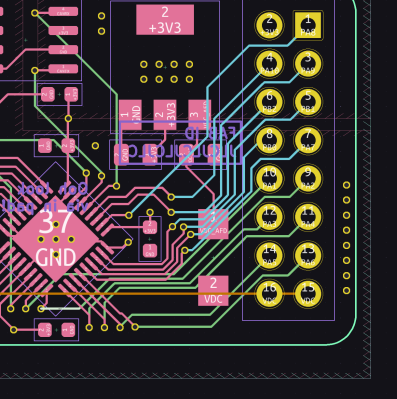
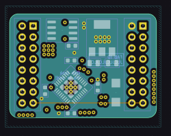
So, how do you do this reroute? Actually, it took me about two or three minutes. First, move In1 tracks to B.Cu using Edit => Edit Track & Via Properties. Then, tweak the now B.Cu tracks to make sure they don’t overlay with In2.Cu tracks. Last step – move In2.Cu tracks to B.Cu using the same menu. Now we have two outer layers that carry tracks, and four layers that are completely empty, save for their fills – a classic arrangement.
Which layers to get rid of? Three of the now-internal layers have GND and one has 3.3 V. You can delete In3 and In4 by changing the board layer count to 4 in Board Setup menu, and decide what to do with the inner layers. There’s two options – SIG-GND-PWR-SIG, or SIG-GND-GND-SIG. For GND-PWR, the 3.3 V plane only wires up three microcontroller pins, but having it as a power plane improves power current distribution somewhat. Alternatively, you could get rid of the internal power plane, for a relatively classic GND-GND inner layer option, and put the 3.3 V pins on B.Cu – thanks to the F.Cu 3.3 V polygon that the board author added, most 3.3 V-connected elements on the board don’t make all that much use of the inner 3.3 V layer when it comes to power delivery.
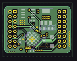
By now, the work is already done, and it only took a short while. With four layers, the board is cheaper to manufacture, especially given that the author already took care to only put components on the top layer – props to them. There’s only a few things left that are of note for me.
Silkscreen, And Some Q&A
The silkscreen of this board could use a few additions, in my opinion. For a start, it doesn’t list the board version, which might just bite you, especially given the internal traces! This is true even more so if you’re making multiples of this board and selling it – it really helps your users to know which exact version of the module they have, so that they don’t have to read chip markings or deduce things by trace layout. My preferred format is %BOARDNAME% by %AUTHOR%, v%VERSION%, and this board could very much use a label like this, given that it’s a module.
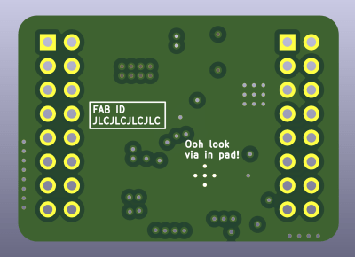
The back of the board is barren, save for the JLCJLCJLCJLC text that safeguards the board’s top layer and a small easter egg. That said, silkscreen is free! There are two options. First option: it could show the module pinout, for the users’ convenience. Second option: it could have some art, for the users’ emotional landscape in one way or another. Choose extra wisely, for both of these choices are wise to make.
Now, here’s a question for the readers – it’s about choosing which components to put onto such a module. This is a board used in an automotive environment – something that is not my domain of expertise, but I’ve read about it here and there, and I wonder if this module would require higher care. For instance, should you put protective elements for the CAN transceiver on this module? CAN termination? Some amount of GPIO protection? Or should these things be relegated to the carrier board, serving as impromptu documentation on the “here’s how you use it” question?
Remember – you, too, can submit your own PCB designs for my review! Send in your board into our tips line, with [design review] in the subject. KiCad is preferred, and a Git repository link desired, but a ZIP file/Google Drive/DropBox link also works. Last but not least, let me know what you think about this feedback, of course – any notes of your own?


“…should you put protective elements for…”
Consider this… an end-user is going to attach this to a vehicle, an expensive piece of equipment no matter where you come from. Do you really want to take a chance on blowing the I/O on what this thing is connected to? Considering you could easily be looking at many $k for replacement modules, I’m going to say a few extra parts on this board are worth the trouble.
My question, if you read a bit further, is whether to have these components on the module vs have them be a carrier board design requirement. I absolutely agree that they should be included, what I’m wondering is, where! What do you think?
If it is on the carrier board then at least some people just won’t add it. If it is on the module then everyone has it. You will probably also get people that don’t know they need to add protection. You could argue that it will say they need to add it in the documentation, but if the goal is to make it is easy and accessible as possible then it should be built in.
Consider the use case for this module. People who don’t want to deal with CAN and want to make it simpler and don’t want to just make their own board, them then having to add components to protect the CAN bus kind of defeats the purpose a bit.
The purpose for this module seems to be for people to just add it to their project and then not have to worry about CAN.
protection diodes and caps to ground on canh/canl where they enter the board, to protect the can transceiver inputs, yeah. There’s dedicated silicon for this in SOT23, maybe SOT523.
The car should already be compliant to automotive standard design, which means that any I/O and power line can sustain quite severe shocks before giving up the ghost. Not saying that you shouldn’t be careful, but in this case it is this CAN module that won’t survive a day in that environment in its current format.
The transceivers are not isolated anyway.i
Two things kind of bother me: First of all the amount / lack of protection also on the voltage regulation. To be automotive compliant a bit more that a linear regulator is needed. Second why choose such an old microcontroller? The F103 is well known, but nowadays I would go for a G431 which also has CAN-FD.
one thing I would change is thermal relieves on the pins. soldering them like this is a pita, desoldering even worse.
oh indeed, I was thinking about this as well, but forgot to note!
Uh where are the CAN termination and bias resistors? Connecting to a car, need CAN common-mode choke as well, and the Vreg looks unprotected for automotive transients. I dislike cute small boards that miss the essentials.
I dislike boards that make assumptions on where I want the CAN termination on my bus/where on the bus the module will reside.
My experience is not with cars but industry, so question: does the ODB-II port assume that a probe connected there has some termination? Given that it is connecting to an otherwise functional CAN bus, I would have assumed there’s already enough termination on the bus. Or does automotive use distributed termination?
EMC nitpicking follows!
The original 6 layer stackup is pretty iffy from an EMC perspective – the return paths for most of the signals connected to the micro are interrupted by routing on the adjacent layer. The STM32F103TB’s GPIOs can (depending on how they’re configured) have rise & fall times as low as 5nS, so even when they’re being used for low frequency purposes they will have non-negligible high frequency energy in their switching edges that will be spread out by the interrupted returns. I wouldn’t expect any functional signal integrity issues in this design, but for this reason alone I would expect to see issues in emissions testing if that ever became a requirement. Arya’s 4 layer stackup is a dramatic improvement in this regard.
On the connectors, I would go as far as placing a GND pin close to every single-ended signal pin to give off-board signals a closer return path. In a design like this where signal integrity isn’t likely to be an issue, “sharing” a GND pin between several signal pins can be a good compromise.
Finally, for EMC bonus points, I would place a GND via adjacent to any signal via where the signal changes physical reference planes. For example, a signal going from F.Cu to B.Cu will have return current going from In1.Cu to In2.Cu; a nearby via between In1.Cu and In2.Cu will keep the total loop area small by preventing that return current from spreading out. As with connector pins, you can compromise by sharing a GND via between signal vias – it’s better than nothing.
I think many of the people writing comments on HaD know a lot more than the people writing the articles…
The HaD comment section is a cumulation of multiple field experts,
Its what you’d expect with any good technical audience, the ability to rip apart a project to pieces, in each reviewer’s specific field of expertise. Some people may take this as being too negative or critical but that’s where the obvious solutions end, and good, real engineering starts.
1++ ….. yep ….. this is a good indication that knowledgeable people are reading and, most importantly, contributing to the article. This is defo no slant on the author – keep up the good work!
Exactly! My favorite comments are where domain experts chimes in. Happens more than you’d expect.
See Maya’s article on route planning: https://hackaday.com/2024/04/04/where-graph-theory-meets-the-road-the-algorithms-behind-route-planning/ just yesterday. [RetepV] worked at TomTom, and has practical insight like only a handful of people on the planet.
And I absolutely second that Arya’s PCB Review series is awesome and informative! And the comments here back that up too.
Ah, the unthinking person’s criticism for when they can’t think up anything valid – “SOMEONE EXISTS WHO IS SMARTER THAN YOU!”
….do you consider that bad?
Arya taught me something new and inspired people who probably do this stuff for a living to share their knowledge, and I learned even more!
Arya’s crushing it.
+1 I am finding most of Arya’s articles most educational and instructional on a practical level.
> Track width is at 0.25 mm by default, but it can go as low as 6 mil
Can you pick a unit of measurement and stick to it – or better still, use BOTH and put one after the other in brackets?
It’s not really possible – this isn’t a case of just not bothering to keep consistent units, it’s a case where the two numbers are coming from completely different parties, and you need to keep them in their native representation to avoid subtle errors.
Kicad works in metric, but the board house publishes it’s capabilities (i.e. the absolute limits for the dimensons they accept) in imperial. It’s only going to cause you to fail board house review if you try to use a metric approximation in the explicit DRC rules and end up with something that violates the real limit.
This will blow up in an actual vehicle. Ldo isn’t enough for this. Load dump or other faults may occur. The CAN isn’t protected or isolated either!
I’m noticing a few comments around the general theme of this being unsuitable for an actual vehicle.
Would be wonderful of those saying such things could add some depth as to why that is the case for those of us who don’t know – and perhaps also comment with solutions, which as I understand it may well be expected to sit on the main carrier board that this module may plug into.
My thoughts there are if it’s going to require or have as a strong recommendation to have protection on the carrier board, maybe that is useful as a note on the silkscreen – point people to an application note, for example?