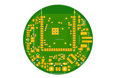
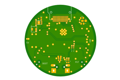
For our next installment, I have a lovely and daring PCB submitted by one of our readers, [Vas]. This is an ESP32-S3 board that also has an onboard round TFT display, very similar to the one we used on the Vectorscope badge. The badge is self-sufficient – it has an ESP32, it has a display, a programming connector, two different QWIIC ports you could surely use as GPIOs – what’s not to love?
This is a two-layer board, and I have to admit that I seriously enjoy such designs. Managing to put a whole lot of things into two layers is quite cool in my book, and I have great fun doing so whenever I get the opportunity. There’s nothing wrong with taking up more layers than needed – in fact, if you’re concerned about emitted/received noise or you have high-speed interfaces, four-layer is the way to go. But making complex boards with two layers is a nice challenge, and, it does tend to make these boards cheaper to manufacture as a very nice bonus.
Let’s improve upon it, and support [Vas]’s design. From what I can see looking at this board, we can help [Vas] a lot with ease of assembly, perhaps even help save a hefty amount of money if they go for third-party PCBA instead of sitting down with a stencil – which you could do with this board pretty easily, since all of the components on it, save for the display, are the ones you’d expect JLCPCB to stock.
Open It Up
The board is designed in Eagle, but I was surprised just how well it imported into KiCad using nothing else but the built-in “File=>Import Non-KiCad Project” dialog. As an Eagle refugee in the past, it warms my heart, because I know Eagle could never reach this sort of featurefulness at the time.
After you import it, open the board viewer and press B to refill the GND zones – the board might look a little scuffed, but I’d be comfortable ordering one for myself as-is! The schematic has imported pretty well too. There are some labels that didn’t import neatly, but there’s nothing I can see that is broken. All the footprint names are present too – helpful for reviewing component choices.
Once again, the board is impressive. I like it a lot – it includes some great features, like ESD diodes on the RST and BOOT buttons for the ESP, separation of the USB VBUS and GND, and a JST-SH power connector for any portable applications. It also has some component choices we ought to discuss.
Component Choices
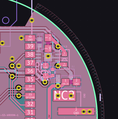
On the left, you can see the two QWIIC connectors that surely work as GPIO expansions in a pinch, and on the right, there’s a JST-PH connector that has power. Next to the QWIIC connectors, you will notice some tiny components – yep, those are 0201 resistors, and there are quite a few of these. The problem with these is that they’re a bother to assemble compared to everything else on the board, they can significantly add to cost if you do PCBA. And they are not even strictly necessary in places where they’re found.
Here’s my take on the resistors. If you are worried that the resistor will interfere with the JST-SH plug being inserted, worry not – this appears to be a footprint for a vertical JST-SH SMD socket, I don’t see how it could be otherwise, considering the 0201 placement. Now, this is not the only place where 0201 resistors are found – let’s take a look at the footprint assignment window for a summary.
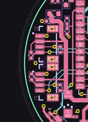
There are some things that immediately spring out. For all 0201 resistors, I’ve taken a look at the board, and it’s not clear to me why they couldn’t be 0402 – especially given how small Kicad’s 0402 footprints are compared to Eagle’s 0402 footprints. Also, I’ve replaced all capacitors 1 uF and lower to 0402, and all capacitors larger than that to 0603. I’ve left some resistors 0603 or higher, in places where it looks like they could be replaced by a ferrite bead in practice, which is what I think was the designer’s intention with both microUSB power/data pins and the 3.3 V input on the ESP.
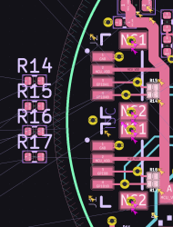
Last thing I will note – it’s not clear to me why I2C bus pullups are different, but I trust the board’s creator. However, 1 kΩ seems way too intense of a value for I2C, from what I’ve seen, especially given so many QWIIC sensors have pullups on them too. So, you could easily replace one of the pullup pairs, or unite them both to something like 1.8 kΩ, the I2C pullup value used by Raspberry Pi with great success, or 3.3 kΩ, the default QWIIC value.
Component Placement
 When I flip this board in 3D viewer (hotkey:F), there’s one thing that instantly comes to my mind, and it’s that the bottom side could be completely clean! In fact, if I understand it right, it’s best that it would be – otherwise, there would be parts under the TFT display, which I feel like would be a mechanical failure point. And parts under the display, there indeed are – at three points, so unless you make a custom standoff or use a healthy amount of foam tape, it’ll be a mechanical bother. Let’s see if we can fix this.
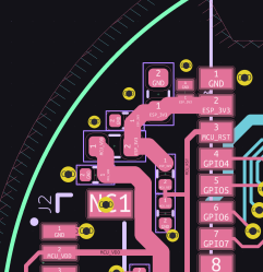
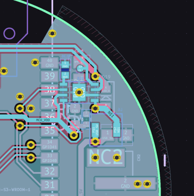
I am surprised to see that Eagle footprints are noticeably larger than their KiCad footprints – specifically the 0402s. On such a cramped board, this really makes a difference, as I will show later. Let’s tackle the top left corner with ESP power filtering first. After replacing the footprints and stacking them closer together, it becomes possible to move the RST capacitor and pullup, freeing up one of the three spots on the back.
 Next, a second spot on the back, near the microUSB connector. First, there are two 0 Ω resistors on the USB pair on the back – with a bit of power trace pushing on the top layer, this is moveable to the front, together with the ESD diodes to ground also on the back layer. The three resistors you can see next to them, however, are a bit of a different story, because they belong to the switching regulator.
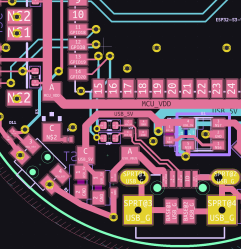
The main problem with the switching regulator section is that the feedback resistors are on the other side. If you’re doing a 2-layer design with a switcher, and this design has two of them, it’s important to provide the switcher with a good ground plane – something that I’m inclined to say feels missing here. However, there isn’t much space – or, there wasn’t, until I replaced the footprints with KiCad ones, and a bunch of space has freed up on the right.
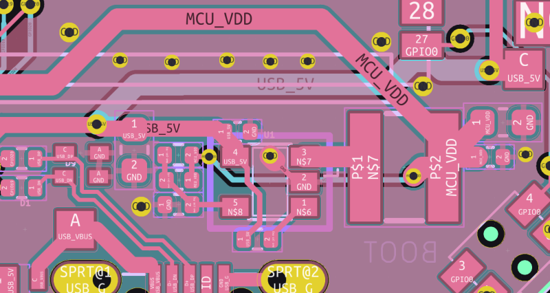
With that space, we can do great things already – but we can free up even more! Here’s something you might notice – there’s no apparent reason why GPIO48 and GPIO45 have to be used, so I opt to remap them to different pins. This lets us remove the entire bottom row of the ESP pads, since there’s no reason to solder to them – this is a good technique if you want to put many traces onto two layers. This lets me replace it with a silkscreen rectangle. This might belong on the Fab layer, but it’s easier for me to hide F.Fab and B.Fab right now to reduce visual clutter, and I need to see this – it can be easily moved later.
 With the free space, we can move power traces to the top, which lets us move the switching inductor and the switching chip to the right – moving the feedback resistors to a top layer, and clearing up the ground plane on the back. Now, the only thing left is the LED driver for the display backlight – just one chip and one inductor.
This is something I’m inclined to leave as an exercise to the reader – I’ve shown quite a bit already. I’m also wondering about the actual characteristics of the display. Does it actually need a boost driver for the LED, or is it sufficient to add a series resistor and power it from the input power rail? If the display has a single-series LED backlight, the driver shouldn’t be necessary, and it isn’t uncommon to drive such backlight using an NPN transistor and a GPIO.
And a last note about something that might bite – the MicroUSB port has a “PCB edge” marking, but it isn’t actually at the edge. This means you can’t use MicroUSB connectors that have “lips”, so you have to watch out that you don’t accidentally buy some of those – they are popular. This is also something that wouldn’t be an issue with USB-C, and manufacturing boards with microUSB in 2024 is a bit passé – but Git says this board was designed two years ago, so I will give it a pass.
Cheaper, Flatter, Lovely As Ever
In all, this PCB review should help decrease the production cost for the board. We replaced 0201 parts with bigger and cheaper parts, united the BOM values, and moved bottom layer parts onto the top layer – at least, most of them, but this should already let us avoid dual-side assembly fees. Cleaning up the switching regulator design should help a lot with electrical noise as well as performance.
I thank [Vas] for sharing this design with us, and I hope that this design got its shot at existence as a real-world PCB already – the round displays are nice to play with, and I can imagine it being a pretty fun badge to wear, especially paired with a suitable battery!


Great article for eagle import.
Watch for antenna keepout as they are meant to stay keepout: even a non-present SD card is a no go! (so are tracks opening the ground of a 2 layers around the antenna)
There is no SD card there. What you see it is the connection for the flex to the display, which makes it also worse, as you have a flexible metal circuit flapping next to the antenna.
But wait, it still can get worse than that too.
If the board is used as a badge, we can presume that the display will point away from the body, therefore the antenna will be sandwiched between a display flex and the body of a person, who is notoriously not the best influence on radio signals.
There is the opportunity here for Hackaday to make another article later on with the polar plots of the antenna in this kind of environment..
In the original version gpio8 and gpio18 have one pullup resistor respectively. In the reworked version, gpio8 has two pullups and gpio18 has none.
Exact!
Great article, there is a lot to learn.
For me it is already a good board, that I can only dream to design :) But it was interesting to read how it could be improved even more.