
Do you have a 5 V device you want to run 24/7, no matter whether you have electricity? Not to worry – Linear Technology has made a perfect IC for you, the LTC4040; with the perfect assortment of features, except perhaps for the hefty price tag.
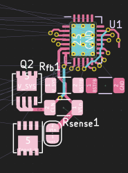
[Lukilukeskywalker] has shared a PCB for us to review – a LTC4040-based stamp you can drop onto your PCB whenever you want a LTC4040 design. It’s a really nice module to see designed – things like LiFePO4 support make this IC a perfect solution for many hacker usecases. For instance, are you designing a custom Pi HAT? Drop this module to give your HAT the UPS capability for barely any PCB effort. if your Pi or any other single-board computer needs just a little bit of custom sauce, this module spices it up alright!
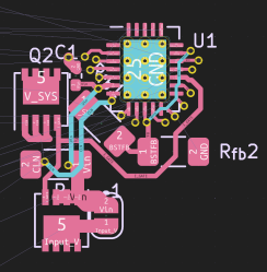
This one is a well-designed module! I almost feel like producing a couple of these, just to make sure I have them handy. If you like the LTC4040, given its numerous features and all, this is also not the only board in town – here’s yet another LTC4040 board that has two 18650 holders, and referencing its PCB design will help me today in this review, you can take a look at it too!
Now, having looked at this PCB for a fair bit, it has a few things that we really do want to take care of. Part of today’s review will be connector selection, another would be the module form-factor, some layout, and some suggestions on sizing the passives – the rows of 1206 components are pretty, but they’re also potentially a problem. Let’s waste no time and delve in.
Battery Wireup And Formfactor
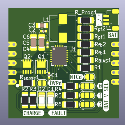
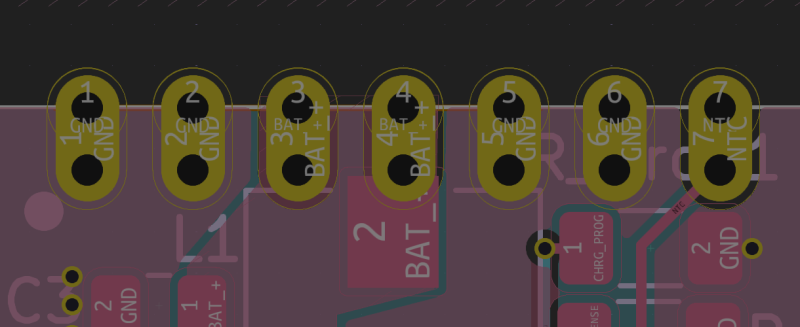
The battery connector uses JST-SH, one pin for VBAT and one for GND. The problem with this is that the module is capable of 2.5 A at 5 V = 12 W. At 3.6 V, that’s 4 A if not more and JST-SH is only rated for 1 A per pin. Using this module with a battery as-intended will melt things. You could add a bigger connector like the standard JST-PH, but that’d increase the module size, and my assessment is that this board doesn’t have to be larger than it already is.
Thankfully, this is an open-source module, so we can change its pinout easily enough, adding pins for the battery into the mix. Currently, this board feels breadboardable, but it isn’t quite – it’s pretty wide, so it will take two breadboards to handle, and a breadboard would also probably be disappointed with the pin amount required. With that in mind, adding pins at the top looks convenient enough.
In general, shuffling the pins around will help a fair bit. My hunch is to make the module’s castellations asymmetric, say, do 7-5-5-5 – one side with seven pins, three sides with five pins. It might not look as perfect, but what’s important is that it will be way way harder to mount incorrectly, something I’ve done with a module of my own design – that was not fun to fix. If you are worried about having enough pins to fill the resulting 22-pin combination, it’s always great to just add GND, doubly so for a power-related module!
Adding more castellations also helps us shuffle the pinout around, freeing up the routing – let’s go through the pins and see what that could help with.
Pinout Changes
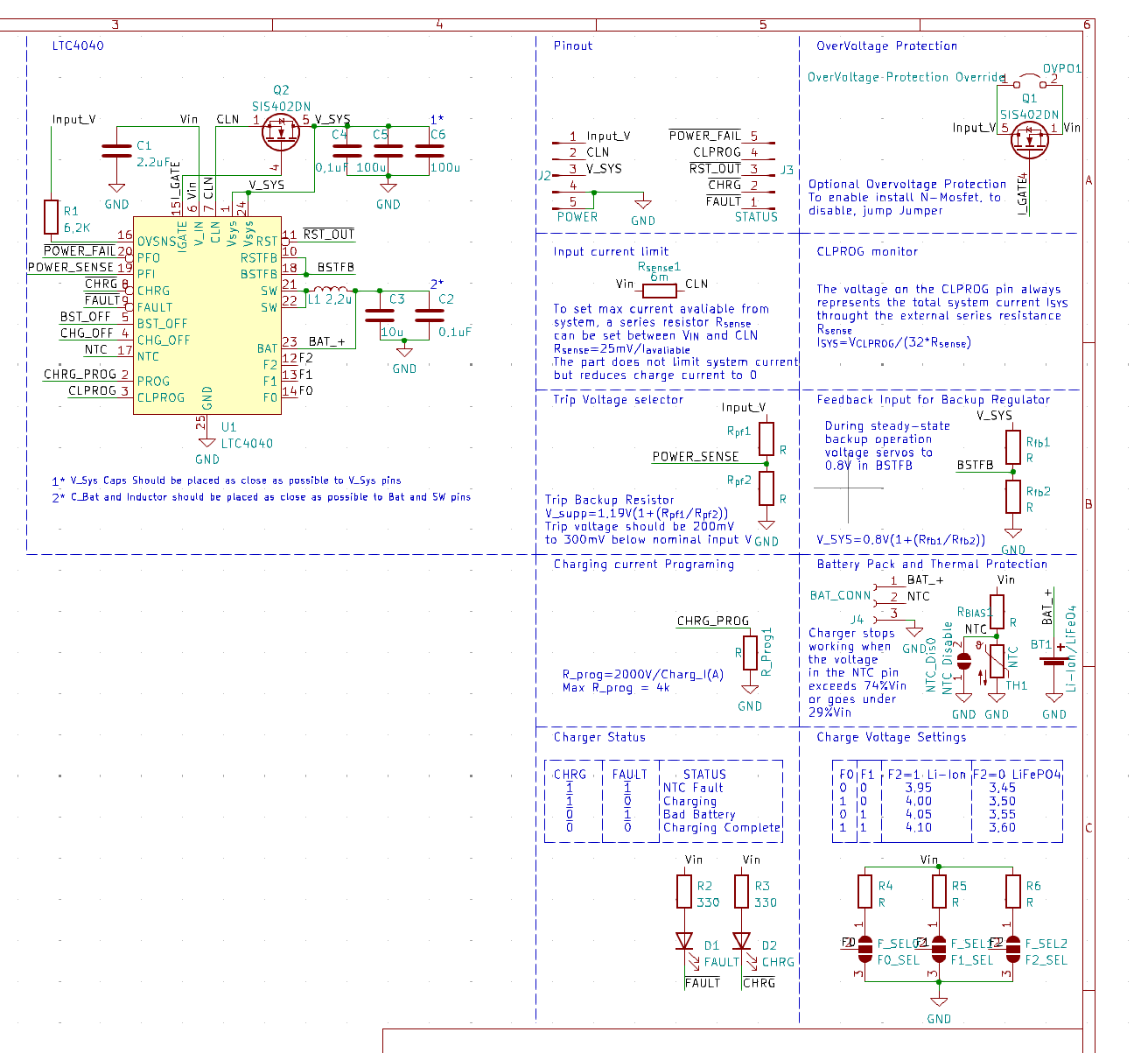 The schematic is seriously nice looking – every single block is nicely framed and has its description listed neatly. Comparing it with reference schematic, it looks pretty good!
There’s a few nits to pick. For instance, BST_OFF and CHG_OFF need to be grounded for the IC to work – datasheet page 10. You could ground them through a resistor and pull them onto a castellation, but you can’t leave them floating. This is not easy to notice, however, unless you go through the pins one by one and recheck their wiring; I noticed it because I was looking at the board, saw two unconnected pins and decided to check.
My hunch is that, first, all the pins were given power names, and then two of them were missed as not connected anywhere, which is an understandable mistake to make.
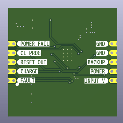
Let’s keep with the schematic style – add two more connectors, one 5-pin and one 7-pin, rearrange the pinout, and keep them in their own nicely delineated area. The 7-pin connector gets the battery pins and a healthy dose of ground, and as for the 5 extra pins at the bottom, they’ll serve as extra ground pins, and give us shuffling slots for pins that are best routed southward.
Components And Placement
Having 1206 resistors on such a module is a double-edged sword. On one hand, given the adjustability, you definitely want resistors that you’d be able to replace easily, so 0402 is not a great option. However, 1206 can actually be harder to replace with a soldering iron, since you need to heat up both sides. The writing is more readable on 1206, no doubt, and it’s also nice that this module is optimized by size. Still, for the sake of routability, I will start by replacing the LEDs and LED resistors with 0603 components – those are resistors you will not be expected to replace, anyway.
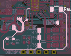 Also, I have a hunch that a few components need to be moved around. First one is the RProg, no doubt – it’s in the way of the switching path, going right under the SW polygon. Then, I will rotate the Rsense resistor so that it’s oriented vertically – it feels like that should make the VIN track less awkward, and show whether there’s any space to be freed on the left.
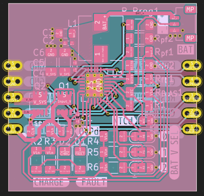
Resistors replaced, a few components moved, and here’s where the fun begins. The IGATE track is specifically designated in the datasheet as pretty sensitive, to the point the PDF talks about leakage from this track to the other tracks – it is a FET gate driver output, after all. Having it snake all around power tracks feels uncomfortable I’d like to refactor these FETs a bit, and see if I can make the IGATE track a bit more straightforward, perhaps also make the space usage on the left more optimized. While doing that, I will be shuffling pins between the castellated edges every now and then.
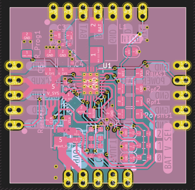
After a bit of shuffling and component rerouting, it felt like I wasn’t getting anywhere. It was time to try and reconstruct the circuit in the way it could make sense, prioritizing the power path and starting with it. For that, I pulled out both FETs, current sense resistor and the feedback divider out of the circuit, and tried rearranging them until it looked like they would work.
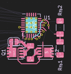
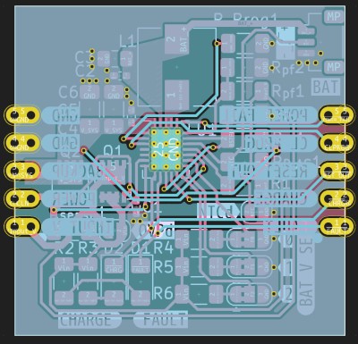
Following quite a few attempts at placing the components, I had to settle on the last one. I_GATE took quite a detour, though I did route it via-less in the end; VIN and CLN went on the bottom layer to give room to I_GATE (and be able to cross each other), and all the non-sensitive signals went into vias so that they could be routed outside of the switching area. It turned out the pinout is seriously not conducive to a neat layout; I suppose, some chips are just like that. Perhaps, it was that the gate driver only could’ve had been located on this particular, so that’s why the IGATE pin is on the opposite side of where the FET could be, instead of it, say, being next to V_SYS outputs.
Post-Redesign Clarity
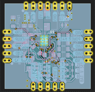
Is the board better now? In many ways, yes; in some ways, no. I don’t know that it’s necessarily prettier, if that makes sense, there were certainly things about the board’s original state that were seriously nice. The package chosen for the FETs definitely didn’t help routing with my I_GATE target in mind, giving no leeway to route things between pins; if I were to change them to DFN8, I could indeed more easily provide a VSYS guard track that the datasheet suggests you use for I_GATE.
I’ve also rearranged the pinout quite a bit. That does mean the STATUS/POWER side distinction of the original board no longer works, but now pins don’t have to go across the board, cutting GND in half. After looking into the datasheet, I didn’t find any use for the CSN pin being broken out, since it’s just a sense resistor net; that space is now occupied by a GND pin, and there’s one less track to route out.
There’s now a good few GND pins on the board – way more than you might feel like you need; the right header feels particularly empty. If you wanted, you could add a Maxim I2C LiIon fuel gauge onto the board, since there’s now enough space in the top right, and quite a few free pins on the right. This would let your UPS-powered device also query the UPS’s status, for one. Of course, such things can always be added onto the actual board that the module would mount onto.
I also removed designators about things that felt too generic – specifically, resistors that only have one possible value and won’t need to be replaced, like LED resistors and pullups for mode selection jumpers. All in all, this board is now a little easier to work with, and perhaps, its ground distribution is a little better.
This module’s idea, and both its authors and my implementation are seriously cool! I hope I’ve helped make it cooler, if at least in the battery connector department. Both the pre-review and post-review versions are open-source, so you can also base your own castellated module off this board if you desire – it’s a good reference design for both LTC4040 and also self-made castellated modules. It’s only 30 mm x 30 mm, too, so it will be very cheap to get made. I hope my input can make this module all that cooler, and, at this point, I want to make a board around this module – stay tuned!
As usual, if you would like a design review for your board, submit a tip to us with [design review] in the title, linking to your board files. KiCad design files strongly preferred, both repository-stored files (GitHub/GitLab/etc) and shady Google Drive/Dropbox/etc .zip links are accepted.


Unfortunately, the price of the LTC4040 is insane. In all my “UPS” needs I went the path of on-line topology with a step-down / charging converter and then a boost converter for the device to be powered. I has some drawbacks too – for instance it is not very power efficient, but using two chinese modules you can construct a good working solution including a reasonably sized battery for the price of the LTC4040 alone.
I wonder how LTC4040 stacks up against XYSemi XR2981 (https://hackaday.com/2024/05/06/upgrading-a-cheap-lx-2bups-ups-board-to-fix-fatal-flaws/). Haven’t had the time to compare the two side-by-side.
That is absurdly expensive (€7.80 roughly)… why not a standard lithium charging chip and a boost chip? I know we’re doubling IC count, but the board would cost a fraction of this.
The problem is that any standard lithium charging IC is just about good at charging, but not at charging AND delivering those 3A for the boost converter. Maybe a diode (or rather MOSFET) based ORing the power rails would work, but meh.
more about the power efficiency and flexibility! though yes, the chip’s mighty expensive
@Arya Voronova said: “Linear Technology has made a perfect IC for you, the LTC4040…”
Linear Technology Corporation (LTC) no longer exists.[1] It has been swallowed-up by Analog Devices Incorporated (ADI).[2]
There is still no really efficient solution for a Li-Ion/Li-Poly 5VDC backup supply in the market, especially when you need to use a 1S backup battery. The battery and backup voltage ranges are just too wide and too low for current technologies. The LTC4040 tries hard, but in the end it just exposes its compromises.[3]
Then when you move to more than one backup battery you run into cell balancing issues. The whole business of simple low-voltage medium to high current DC power system management and backup remains an area seeking a better solution than what is available today – and it goes far beyond just PCB layout.
* References:
1. Linear Technology
https://en.wikipedia.org/wiki/Linear_Technology
2. Analog Devices
https://en.wikipedia.org/wiki/Analog_Devices
3. LTC4040 @ ADI
https://www.analog.com/en/products/ltc4040.html
it’s a product designed by Linear Technology, not Analog; Analog has purchased Linear later on. Also, I don’t see how “in the end it just exposes its compromises.” is supported by your link, could you please elaborate?
Arya Voronova said: “I don’t see how “in the end it just exposes its compromises.”
Simulate the LTC4040 in LTspice and run it as a 1S UPS over a 2.7-4.2 VDC battery range at a couple of amps. Working from memory, the resuls were rough. The power path is not too bad, but the up-conversion needed work. I think I replaced the LTC4040 with a PMOS (or two) for the power path switch and a SEPIC converter. But even that attempt had start-up and stability issues. Switching to a 2S battery helps, but balancing a 2S battery comes with challenges of its own.
Ahha, that makes sense! One nit to pick – I wouldn’t expect reasonable performance below 3.3V for a LiIon cell.
This is interesting as always, thanks Arya!
Heads up – most of the images I can click to get a bigger version, but not the schematic. It’s a little hard to read at the embedded size.
By magic: https://hackaday.com/wp-content/uploads/2024/05/hadimg_desrev_ltc4040_6.png :-)
Thank you! ^_^
Oh that’s weird, I specifically aimed to make it clickable; perhaps I chose the wrong option, gonna fix!
What’s your thoughts on a pin spacing of 3.62mm for castellated boards like this? That’s 2.56mm * sqrt(2).
See where I’m going with that?
A small board like this with that spacing could go diagonally on a breadboard, and with the right placement and counts, still leave enough sockets on the breadboard lines to connect up jumper wires. Pins would need to be soldered on individually, or possibly in pairs, which makes it a little more difficult, but using as a stamp with custom pad spacing is still possible.
I like the sentiment, but I would be going nuts trying to figure out why the hell they weren’t 2.54 spaced, and not knowing the 3.62 was the actual magical number.
Rotating components and labels 45 degrees might help.
Also, route as many tracks as possible at 45 degrees.
Oh that is an interesting idea! Wwith five rows for a breadboard, you’d be limited to like 4 pins per side before you ran out of space to plug jumpers in, but I can see it working out for a certain type of module, especially given this enables a 4-sided castellated stamp to be breadboarded fully.
Quote: “The schematic is seriously nice looking – every single block is nicely framed and has its description listed neatly.”
Really?
I find the schematic horrible. It’s got loose resistors everywhere, hidden in small text boxes and you have to follow labels to see how the feedback circuit is actually connected to the IC. The resistors for the voltage dividers also don’t have values in the schematic. There is just a generic formula to calculate them. The total resistance of such a divider is also important.
Putting everything in small boxes in a schematic seems to be a new trend but I don’t like it at all. It mostly obfuscates connections.
Just try to follow the (high current) path from the input connector (already hard to find on the schematic) to the output (wherever that is). Even single resistors such as a current shunt is broken out with labels and hidden in some text. It’s very difficult to get an overview of how this IC works and how parts relate to the IC without reading texts.
There is also far too much text in the schematic. It is nice to have documentation with the schematic, as a sort of datasheet or notes for the project, but this should not in the schematic itself.
And what’s the chinese equivalent?
Really nice and Thanks for making all the changes and pointing all the things that can be improved. I did this back in time to learn how to route buck and boost converter circuits, but at the end I ended rushing it a bit, and didn’t think to much about for example the connector to the battery
Are the files anywhere to be seen? I would love to point the repo to your new design (So they don’t take mine by mistake) and maybe make myself two of this boards (I have two samples of the chip and the corresponding coils with me)
Is this what you’d use for any portable design that you’d want to be able to plug in and charge? I’ve been curious how to make a proper design for plugging and unplugging a charger while otg.
Is this topology/chip only used for UPS and shouldn’t be used for a portable laptop-like device battery?
BQ24610 is a much more flexible and affordable way to achieve the results. The only flaw is the PCB size, it will be larger but not too much, with the reasonable external components choice