
Today is another board from a friend, [treble], who wants to convert a Yaesu FRG7700 radio to USB-C PD power. It’s yet another review that I’ve done privately, and then realized I’ve made more than enough changes to it, to the point that others could learn from this review quite a bit. With our hacker’s consent, I’m now sharing these things with you all, so that we can improve our boards further and further.
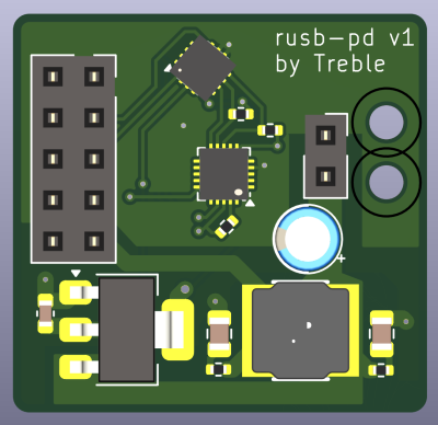
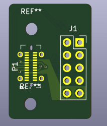
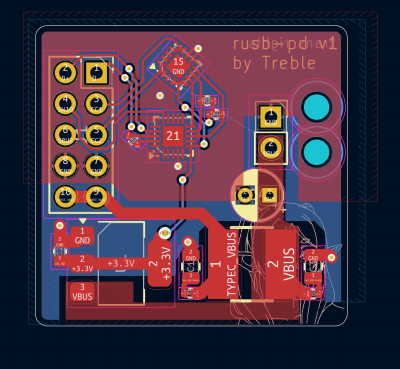
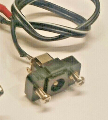 This board’s idea is thought-out and executed well – it replaces a bespoke barrel jack assembly, and is mechanically designed to fit the screw holes and the free space inside the chassis. For USB-PD, it uses a CH32V003 coupled with FUSB302 – I definitely did help pick the latter! For mechanical reasons, this board is split into two parts – one has the USB-C port, whereas the other has the MCU and the PD PHY.
In short, this board is a PD trigger. Unlike the usual PD triggers, however, this one is fully configurable, since it has a 32-bit MCU with good software support, plus, the PD PHY is also well known and easily controllable. So, if you want special behavior like charger-power-dependent profile selection for powering a static resistance load, you can implement it easily – or, say, you can do PPS for variable voltage or even lithium ion battery charging! With a bit of extra code, you could even do EPR (28 V = 140 W power) with this board, instantly making it into a pretty advanced PD trigger, beyond the ones available on the market.
Also, the board has some PCB art, and a very handy filter to get some of the USB-C charger noise out. Let’s take a look at all of these!
Current Flow Improvements
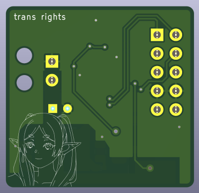
First of all, the back of the PCB has art. This is a problem. Specifically, the art has to be bigger. See, fabs might struggle drawing thin silkscreen lines. So, I will take the liberty of enlarging it. This board is 25×25 mm in size, after all. Due to the way KiCad works, I’ve had to ask for the original .svg file from [treble] for that. Here’s a tip that I myself should follow more, if you’re adding PCB art, storing its sources alongside the board is pretty valuable for whenever it might need to be regenerated or modified!
This board is seriously nice. It has thick traces for power, and, it makes liberal use of filled zones for higher-current tracks, too! It’s not often that I see these fills used, even for higher-power areas, and truth be told, I get lazy to draw them, but they are possibly the cleanest choice for a board that fulfills a power-related purpose. Also, as usual, it’s just two layers, something dear to my heart.
Now, let’s take a good look at the two layers we have. This is a board that current is supposed to flow through, and if you have an eye for it, you might notice that it will be impeded more than you’d want it to be, in ways that are easy to fix.
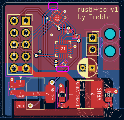
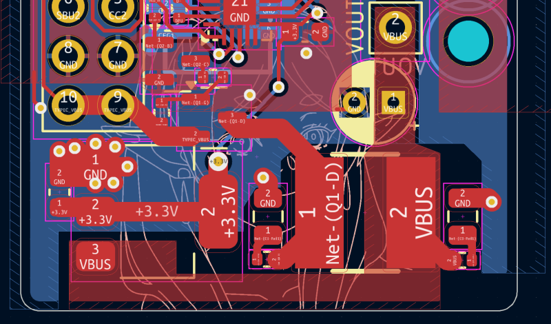
Take a look at the board’s bottom layer. It has a ground plane, yes, but there are also tracks going all across it. If you try and visualize the way that ground return current could flow across the board, you might realize that it has to go through a few small slivers of copper; this is despite the ground fill being present on both sides. Let’s fix this.
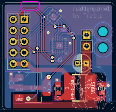
Here are three spots where you could straightforwardly add ground connectivity purely by moving vias. I usually look out for such spots as part of my after-design cleanup routine – something I might spend a good half an hour on; just, idly glancing at the board in the 3D viewer, looking here and there, trying to notice any things I could improve upon. Here, if you wanted a high return on your investment, you could move these vias and gain whole two new paths for ground return current to flow through.
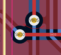
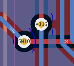
Moving tracks around will yield way bigger returns for freeing up some ground area. For a start, the SWIO pin, wittily wired up to an SBU pin on the USB-C connector with the trace snaking between the 2.54 mm header pads, doesn’t have to go on B.Cu at all. The VBUS connection of the FUSB302 could also be moved to the left edge, all around the 2.54 mm connector, so that it doesn’t have to cut the ground polygon in half. Furthermore, we could improve upon USB diffpair routing by rotating the CH32V003 90 degrees clockwise, and having the pairs go back onto the front layer again at the top. Part of the 3.3 V track could be routed on the top if you rotate a resistor 180 degrees, and voila, we now have a healthy and plentiful ground polygon.
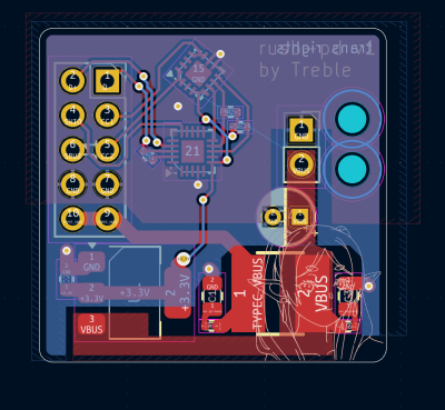
“Route as much of your board on a single layer as humanly possible” is still a great guideline, and it helps here, too. It also helps if you look at your board and visualize the way that ground return current will flow, from one side to the other, all along the signals.
Only a few small details are left. The ICs don’t have decoupling caps on their 3.3 V inputs, and we could easily add them – cleaner power is always a plus. Oh, and the linear regulator could use a couple more vias from its GND pin – purely for the heat dissipation potential. There’s a 1.5 K resistor used for a USB pull-up, and I2C uses 3.3 K pullups in the same package – I’ve changed them to use 1.5 K too, just as a BOM optimization reminder; should work wonders for I2C.
Implementation Details And Polish
Something I don’t expect hackers to know but is nice to keep in mind – the VBUS pin of the FUSB302 is fault-prone and PSU noise on it can cause the FUSB to die in a way that short-circuits the 3.3 V rail, to the point that the Pinecil soldering iron eventually disconnected it in a new hardware revision, and the community has developed guides to disconnect the VBUS pin. Furthermore, the VBUS connection on the FUSB is not even needed for any part of the PD process; essentially, it’s not even a nice-to-have, all you get is an interrupt that doesn’t carry any meaning in our “bus-powered” arrangement. Let’s disconnect it – that frees up quite a bit of ground and routing space around the FUSB302.
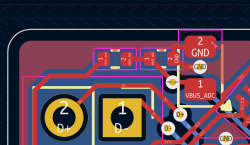 Now, adding a 1:10 resistor divider to an ADC-capable CH32V003 pin would be worthwhile – this lets us measure the voltage we get, checking that it’s indeed the voltage we need. FUSB has provisions to measure voltage on its VBUS pin, but they’re bothersome to use, using an on-MCU ADC is way easier. I’ve also added a 3.6 V Zener diode in 0805 package, clamping the voltage that reaches the GPIO – I don’t expect it to actually be needed, but we do have space for it, and it protects the MCU’s GPIO in case of any assembly errors or voltage spikes; I have previously mis-placed a resistor at a voltage divider, and now I’m worried about others doing it. Worst case, the Zener doesn’t have to be placed at all, and you can just add a capacitor there, smoothing the divided voltage before it reaches the ADC.
What else? Here’s something to consider – the radio might not be happy with 5 volts on its power input, which is an inevitability given how the USB-C negotiation process works. Remember, first, you get 5 V, and then you have to negotiate further up. This is why PD trigger ICs tend have a PG pin, that you can connect to a P-FET gate, and that pin is only driven after a successful negotiation. In our case, we have MCU GPIOs we can use instead!
With an NPN driver and a provisional 3:1 divider for the gate voltage, the “power good” circuit fits into the board space wonderfully. If it’s not needed, it can be easily jumpered with a 0 R resistor across the FET pads, but adding this circuit retrospectively would be bothersome – it helps that we have the footprints for it. Remember, traces and footprints are free to add, fundamentally – just like silkscreen markings.
How Will You Use Your Board?
Another great thing to visualize is – after you assemble your board, how will you interact with it? Here, [treble] still has to write the USB-PD firmware – in C++, no less, my MicroPython stack won’t be directly applicable, as much as I will help, but [Ralim]’s open-source PD stack used in the Pinecil could work wonderfully! While integrating that, she will have to debug things. Possibly, might even have to debug it some more later on, with the board installed into the radio chassis. It’s a project one hacker could pull off without a doubt, and, there’s things you could add to your board that will help.
The SWIO pin of the CH32V003 goes to an SBU pin on the USB-C socket. This is a great decision, because you can easily reflash the MCU without disassembling the entire radio – just have a USB-C plug with SBU exposed and that’s enough. Also, when I’m thinking about it, it might be troublesome during active development, because [treble] will have to constantly unplug and plug the PSU and the programming plug while debugging the in-progress firmware. Now, she could solder to the 2.54 mm pin headers, sure – alternatively, you could add an extra SWIO header at the edge and make her job a bit easier. I can’t find much space for it, sadly, so I suppose a female header with longer male pins (Arduino and Wemos shield style) can do just as well, also allowing to probe CC pins as a bonus.
I feel like there’s a good few more things you can add to improve development and usage comfort. Will there be a failure mode where the board has to signal to the user that something’s gone wrong – say, with a 5 V USB-C PSU inserted? Let’s add two LEDs on one pin – could even do WS2812 sometime later. What about I2C communications, what if tapping them would be useful during the board’s development? Let’s add a QWIIC socket and pull the I2C lines onto it – not for expansions, but rather, so that you have a socket you can easily wire up to a logic analyzer, plug it in and unplug it at any point.
There’s some arguments to be made for breaking out as many CH32V003 pins as possible. I will refrain from it, as much as it’s tempting – at this point, there isn’t a lot of board space in the spots where it matters. It would be cool to have them on testpoints though! Speaking about that, I’ve just realized – you could add a tiny SMD three-position DIP switch onto the back of the board reasonably easily, so that you can have “profiles” for the trigger board, CH224 PD trigger board style. I’ve found the tiniest three-position SMD DIP switch that LCSC has, then added it to the back of the board, trying to still have the ground fill as intact as possible – the idea is that this is a nice feature for whenever the board might be used as a more general-purpose trigger board. When not populated, it serves as a breakout for three ADC-capable GPIOs, GND, and 3.3 V!
Now, I’d like to emphasize: the DIP switch is not exactly necessary in this project. It falls into “something that’d be cool to fit in space left over, if the board is to be used in an entirely different setting”. Overall, I try not to push features this remote onto people while doing design review – plus, it does clash with the silkscreen. So, this addition is easily removable from the PCB files, and it doesn’t have to be populated either. Also, I’ll stop the additions here, to avoid feature creep.
That about wraps it up for things I feel like this board needs. Let’s talk about an aspect where I’d like your opinion.
Questions For The Audience
Now, here’s a question for the audience, on two things I’m not well-versed on. First one is – here’s a Pi filter. The purpose is filtering out 300 kHz USB-C charger switching frequency that [treble] has noticed being produced by a USB-C charger she’s picked. Having simulated this filter in LTSpice, it appears to be good for filtering out 200 kHz and above. Does that look correct? And, any things she should look out for when it comes to component choices?
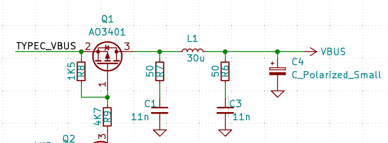
Another question is – the ground cutout under the Pi filter. My understanding is – the more ground, all over the board, the better. [treble] decided to remove ground under the Pi filter, as far as I recall, due to a gut feeling that it’d decrease noise imposed by the inductor. Does that make sense? I’m tempted to say “no”, but I can’t formulate a good enough explanation on the specific downsides and how it might need, which is why I’m asking you.
Another board reviewed, and due to the way it’s built, I can easily imagine ordering a dozen for use in my own projects – thanks to [treble] for sharing this, and I hope this feedback helps! As usual, if you would like a design review for your board, submit a tip to us with [design review] in the title, linking to your board files. KiCad design files strongly preferred, both repository-stored files (GitHub/GitLab/etc) and shady Google Drive/Dropbox/etc .zip links are accepted.
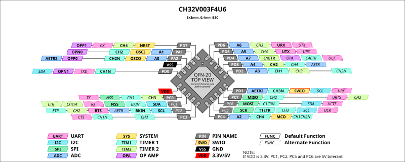
I thank [Julianna] for helping me check the the CH32V003 circuit!


“…ground cutout under the Pi filter…”
If the inductor is shielded, it will have no practical effect upon the ground plane. Given this is a typical popcorn component (and no BOM to verify), it’s likely not a shielded type, so that argument alone is irrelevant.
If it’s not shielded, you will have some amount of mutual coupling to the ground plane. BUT, the coupling will be quite poor, so the induced current in the ground plane will be very small (which means the induced voltage will also be very small). “Small”, of course, being relative… but in this case small enough that your typical home lab test equipment couldn’t measure it (and therefore negligible to the point of “don’t care”).
In short, cutouts of the ground plane under the inductor isn’t going to do anything for you as there’s already a lack of problem in the first place.
Thank you, this makes sense to me!
It’s also good to compare the effect that adding a cutout has in terms of breaking up a ground plane; a heavily cut up ground plane can have resonant modes / function less well as a ground plane. In some cases there is enough noise coming from a component to justify removing it, but usually not.
I’ve heard of removing ground for the switching inductor on a DC dc converter, but even that often isn’t needed. For use as a filter, I would keep the plane.
Yeah, I don’t see it done anytime often either, gotta admit.
Notably, the circulating currents – and associated potential differences – will be nowhere critical. There is no noise sensitive part next to it which could pick it up.
On the other hand, the gap significantly extends the loop area. The (dampened) oscillations in the PI filter will have to go all around the VBUS pin on the header.
And speaking of resonances, the PI filter is actually *resonant* at 300kHz. The reason the whole circuit is not resonating is the electrolytic cap next to it. I would recommend increasing the MLCCs to 330…1000nF, and lowering the resistors to 10…22 Ohm.
Probably, start the layout from scratch – put the MOSFET and filter in the lower left, shortening the trace length. Put the linear regulator in the bottom right corner, so 3V3 does not have to cross VBus, route 3V3 along the right edge of the board. Probably replace the LDO in the large SOT-23 package with something smaller.
Why is Frieren on this board? Cause they felt like it or is there some joke I’m missing?
IIRC, just silkscreen art – silkscreen art is good! This particular snapshot was a meme for a while, so it made its way onto the board eventually, too
Your P-fet for the reverse polarity protection circuit is the wrong way round. It has to be reverse biased. Drain is input, Source is output.
Oh this is not reverse polarity protection, this is specifically protection against letting the before-negotiation 5V go onto the circuit’s output to the radio, with the FET being switched by the MCU! And, thank you for taking care to point it out ^~^
Is there a semi-standard way to note things like that? Even in the schematic, if not in the silk?
Since you’ve removed my completely inoffensive comment i’ll assume the best in that you just misunderstood.
I’m not criticising your particular brand of politics i’m just saying that it’s not appropriate to insert any political messaging in this context.
Discussing that is not the purpose of this article. I’ve seen these discussions online time and time again, and they always go nowhere, except for one point that always remains. You can’t dictate what messaging other people put onto their PCBs or other creations, that is simply not up to you or anyone else, except the person creating it. Most you can do is choose to associate or not associate with that person based on their messaging. That’s as far as this discussion will go. If you want to contribute to this comment section, I do invite you to comment on something else, because I’ve seen this one way too many times, and reviving that debate yet again every time someone sees a board have text on its silk is just going to give me whiplash =D
edit: as much as a stack of meta-level conversation about may be tempting, I do write these articles so that the design and its improvements can be discussed on their merits.
Hear hear.
Should this article be tagged “design review”?
indeed, done, thank you ^^
Glad to help.
Even though your inconditionnal love for 2 layers boards is beyond sanity, I must say your articles are probably the best I read on hackaday these days, thanks!
I find it unusual to see resistors in the Pi filter, but for low frequencies it might ease up on the Capacitor size and if an LTSpice simulation is showing the proper cut off it should be fine.
My general rule of thumb is do not split up ground planes unless you are breathing electro magnetic field theory. Done it on some pcbs and regretted it during emc testing.
The issue here is, that noise from a power supply usually creates noise on both supply and return path aka GND. Since the filter is only in the supply path splitting up the ground plane is most likely not useful. To prevent noise from the power supply I would recommend using a common mode chocke. If you use a common mode chocke it makes sense to split up your ground plane, because every bit of current has to go through the chocke.
Why are you worried about the split ground plane? If it is aesthetics, then cool, valid choice. But if it is about signal integrity, how do you know the changes were a net benefit?
A more solid plane is good, but the signals themselves are all still jumping gaps, and now the differential pair is going through extra vias. On the other hand, maybe signal integrity isn’t even a priority, because (after the board is working) you won’t be sending through much data.
In which case, maybe you want part of the board to be a power plane, or at least a power finger. Looking at the middle version, I might even have been tempted to put power instead of ground under the chips’ thermal pads, if I were sure they weren’t electrically connected to ground inside.
Come to think of it, is that companion board a standard breakout you already have several of? Because otherwise, why not just rearrange the pins there, so none of your incoming signals have to cross each other?
Could someone explain a little more about VBUS in this design? I’m pretty sure at least some of my assumptions are wrong, but I’m not sure which ones.
As best I can tell, the original board takes in TYPEC_VBUS, and sends it to a chip (power supply?) on the bottom right, which then sends the conditioned power out as VBUS, including to the FUSB302B chip’s VBUS pin.
The FUSB302B uses that to tell whether/when the other end of the USB cord is attached. I think this is the message that Arya called “not even a nice-to-have” for this design. It would go off when VBUS passes through either the Bus threshold (VBUSOK) or maybe 4.5 V (I_VBUSOK).
I think it also measures the voltage of its input, which might be one reason to pass it the already-conditioned power that the radio would see, though Arya prefers the other chip for that. I assume most of the power is going out through the pair of through-holes on the right, to power the actual radio.
By the middle design, TYPEC_VBUS is no longer connected to VBUS. I assume this is bridged by one (or both) FETs, but I don’t really understand how, nor do I see how two are better than one.