While low-cost professional PCB fabrication has largely supplanted making circuit boards at home, there’s still something to be said for being able to go from design to prototype in an afternoon. Luckily we aren’t limited to the old toner transfer trick for DIY boards these days, as CNC routers and powerful lasers can be used to etch boards quickly and accurately.
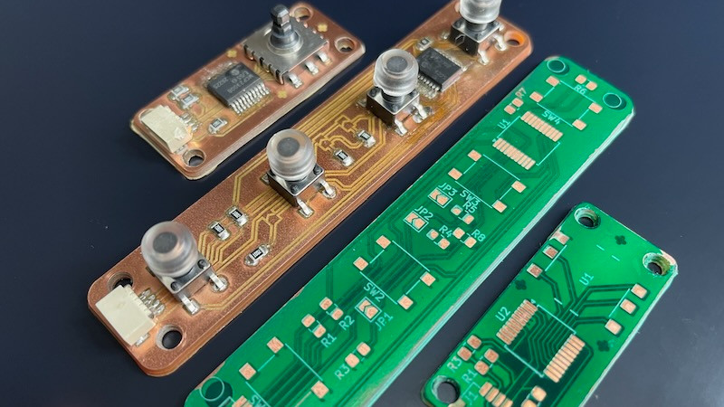
But there’s still a problem — those methods leave you with a board that has exposed traces. That might work in a pinch for a one-off, but such boards are prone to shorts, and frankly just don’t look very good. Which is why [Mikey Sklar] has been experimenting with applying both a soldermask and silkscreen to his homemade boards.
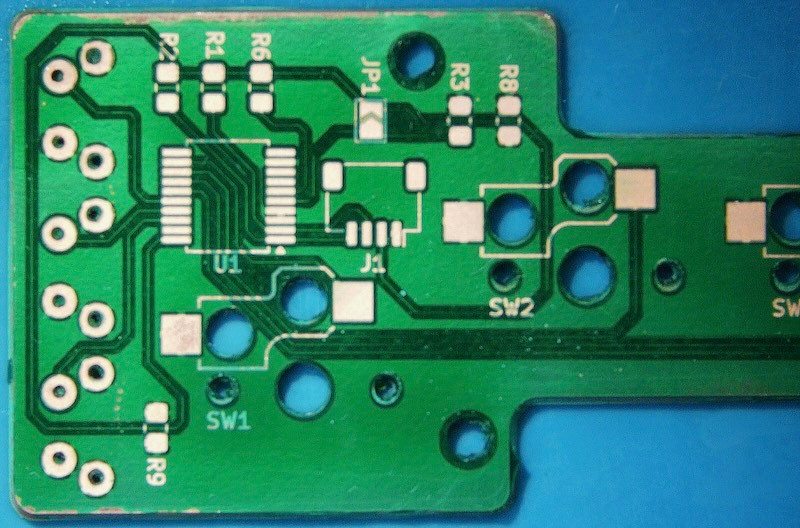 The process he describes starts after the board has already been etched. First he rolls on the soldermask, and then sandwiches the board between layers of transparency film and clear acrylic before curing it under a UV light. After two coats of the soldermask, the board goes into a fiber laser and the silkscreen and mask layers are loaded into the software and the machine is set to a relatively low power (here, 40%). The trick is that the mask layer is set to run four times versus the single run of the silkscreen, which ensures that the copper is fully exposed.
Since the board doesn’t need to be moved between operations, you don’t have to worry about the registration being off. The end result really does look quite nice, with the silkscreen especially popping visually a lot more than we would have assumed.
We’ve previously covered how [Mikey] uses his CNC router and fiber laser to cut out and etch the boards, so this latest installment brings the whole thing full circle. The equipment you’ll need to follow along at home isn’t cheap, but we can’t argue with the final results.


The results look amazing!
Double sided, plated through holes?
Obviously not.
Hijacking topic :) My 4 year old experiments, but more details how to prepare files and laser parameters: https://www.kurokesu.com/main/2021/01/07/making-fine-pitch-pcb-prototypes-with-fiber-laser/
Thanks for the writeup. I skimmed through, your boards look great as well. I see in the comments that you were also working on punching holes for vias using the laser. Did you make a follow-up post about that?
So what’s the conductivity of FR4 when you pyrolyze the top few microns with your laser?
Paying 10$ and waiting for a week for my PCBs to arrive from China. Or paying several thousands of dollars for a fibre laser and the setup to make everything work, and save a few days worth of time.
The answer is obvious. The latter
Thousands of open source designs online, AI-assisted modifications, cheap PCBs with assembly, cheap 3D printing services. Hackaday visitors are secretly being turned back into consumers!!
Do you make your own shoes?
Actually – not obvious. It depends on how many PCBs you need and with what tolerances. And how quickly.
It looks amazing, really! If only those fiber lasers would not cost thousands of dollars yes.
Meanwhile I will stick to low cost cnc/laser and what can be done with it https://hackaday.io/project/195654-print-your-own-pcbs-with-lasercncchemicals
Although it’s tricky to work with, you still have drilling holes and engraver in one machine.
Maybe a fine-nozzled lower pressure water jet CNC cutter could be used to both etch the copper out from FR4 and drill the holes in one go?