Intel’s 386 CPU is notable for being its first x86 CPU to use so-called standard cell logic, which swapped the taping out of individual transistors with wiring up standardized functional blocks. This way you only have to define specific gate types, latches and so on, after which a description of these blocks can be parsed and assembled by a computer into elements of a functioning application-specific integrated circuit (ASIC). This is standard procedure today with register-transfer level (RTL) descriptions being placed and routed for either an FPGA or ASIC target.
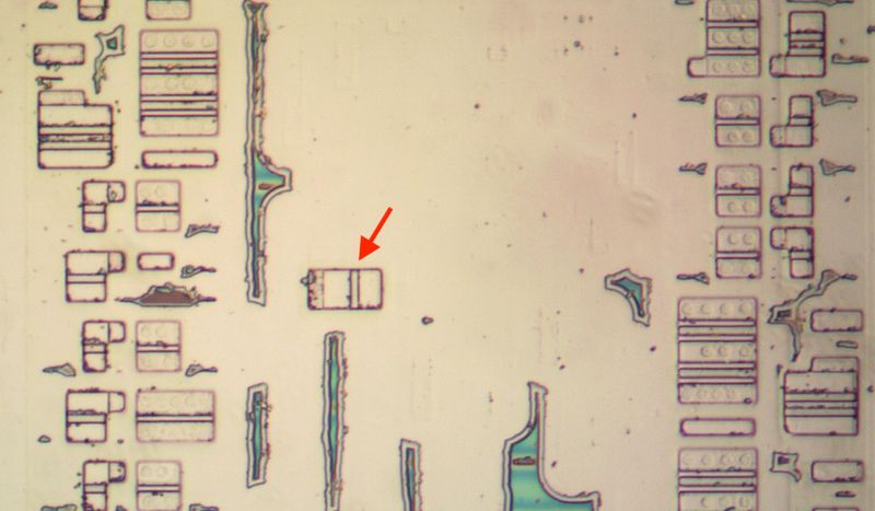
That said, [Ken Shirriff] found a few surprises in the 386’s die, some of which threw him for a loop. An intrinsic part of standard cells is that they’re arranged in rows and columns, with data channels between them where signal paths can be routed. The surprise here was finding a stray PMOS transistor right in the midst of one such data channel, which [Ken] speculates is a bug fix for one of the multiplexers. Back then regenerating the layout would have been rather expensive, so a manual fix like this would have made perfect sense. Consider it a bodge wire for ASICs.
Another oddity was an inverter that wasn’t an inverter, which turned out to be just two separate NMOS and PMOS transistors that looked to be wired up as an inverter, but seemed to actually there as part of a multiplexer. As it turns out, it’s hard to determine sometimes whether transistors are connected in these die teardowns, or whether there’s a gap between them, or just an artifact of the light or the etching process.


“application-specific integrated circuit (ASIC)”
Thank you thank you thank you thank you infinity for defining an acronym, as writers are supposed to do!
Looking at you other HaD writers.
+1
Err…
I would like to know based on what method you gained inside into this transistors , did you used a delayer technique ?
I posted a snarky comment recently, although I think it may have been on Reddit? Anyways, I looked up the world’s longest acronym. From the USSR(of course)54 Cyrillic letters, 56 when transliterated into Latin alphabet. I’m not going to repeat here, but it proves acronyms can get really out of hand! Engineers love them, in the military, government and civilian computer geekdom (after all, right after WWII, these were often the same people!). But there’s little effort in writing out the full name at least once per article. A friendly reminder to do so is a good thing.
Neither PMOS and NMOS was spelled out, but as adjectives of “transistor,” I don’t think it was necessary.
From the cited article: “Multiplexers in the 6502 use a single NMOS transistor, rather than the two transistors in the CMOS switch. However, the performance of the switch is worse.” That’s only true sometimes. In silicon, PMOS transistors are only 1/3 as strong as NMOS transistors of the same size. That means that for a switching threshold of half the supply voltage, PMOS transistors need to be 3X as large as NMOS transistors. 3X as large means 3X the capacitance, and capacitance is what slows down a circuit. On the other hand, NMOS transistors aren’t good at pulling voltages high, so there’s a tradeoff involved.
Most standard cell design is static CMOS. Static means the clock can stop and everything retains its logic state. Static CMOS design is relatively easy and dependable, but it’s also the slowest. There are a number of MOS design strategies that are much faster, using dynamic circuits and trying to have mostly NMOS in the signal path. These strategies can be difficult to use, especially in a large complex IC. In dynamic logic there’s a minimum clock frequency below which logic states may be lost.
I’ve been out of the field for 24 years now, so maybe some of the above is no longer true.