Getting PCBs made is often the key step in taking a dodgy lab experiment and turning it into a functional piece of equipment. However, it can be tedious to wait for PCBs to ship, and that can really slow down the iterative development process. If you’ve got a 3D printer, though, there’s a neat way to make your own custom PCBs. Enter PCB Forge from [castpixel].
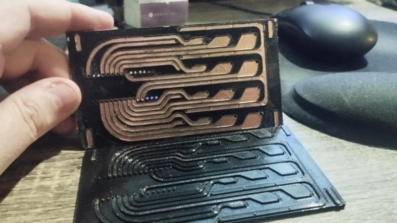
The concept involves producing a base and a companion mold on your 3D printer. You then stick copper tape all over the base part, using the type that comes with conductive adhesive. This allows the construction of a fully conductive copper surface across the whole base. The companion mold is then pressed on top, pushing copper tape into all the recessed traces on the base part. You can then remove the companion mold, quickly sand off any exposed copper, and you’re left with a base with conductive traces that are ready for you to start soldering on parts. No etching, no chemicals, no routing—just 3D printed parts and a bit of copper tape. It rarely gets easier than this.
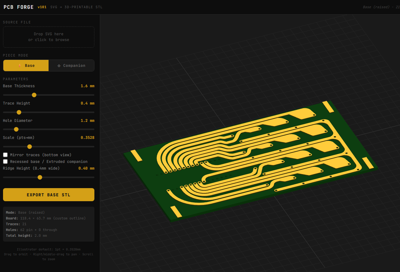
You can design your PCB traces in any vector editor, and then export a SVG. Upload that into the tool, and it will generate the 3D printable PCB for you, automatically including the right clearances and alignment features to make it a simple press-together job to pump out a basic PCB. It bears noting that you’re probably not going to produce a four-layer FPGA board doing advanced high-speed signal processing using this technique. However, for quickly prototyping something or lacing together a few modules and other components, this could really come in handy.
The work was inspired by a recent technique demonstrated by [QZW Labs], which we featured earlier this year. If you’ve got your own hacks to speed up PCB production time, or simply work around it, we’d love to know on the tipsline! Video after the break.
Due to popular demand, here is a demonstration video of how to make 3D printed PCBs using just vector drawing software, a 3D printed (PETG filament for mine) and self-adhesive copper tape. Any questions, let me know!
— castpixel ⚧️⚢ (@castpixel.bsky.social) 2026-02-19T14:15:42.137Z


This is one where I would like to see a video for once. Primarily of the filing step. The end result looks great, the idea is also cool. How they got it to look so clean filing away sticky copper tape is the surprising part to me.
Not filing. Sanding. That’s a world of difference
It’s really not all that much different they’re both removing materials files are more consistent sandpaper not so much but it’s pretty much the same concept and usually you can use a needle file anywhere you could use sandpaper.
It’s meaningfully different in this case, as the sanding most people will be doing less aggressive and more manageable than using a file on adhesive backed foil.
This is an obvious implementation quirk, don’t get caught up on definitions.
Video here: https://bsky.app/profile/did:plc:oybl65tqxhrz2kudyddnfsll/post/3mf7rsdcwq22h
Only demonstrates manufacture of the ‘PCB’. Does not demonstrate any soldering.
FWIW, do not see any advantage in this method for either cost or time or materials over traditional PCB etching. And the use of STL for PCB layout is inefficient.
It doesn’t need chemical etching.
Qzw labs demonstrated soldering pretty convincingly, on PLA no less.
So I didn’t think people would need convincing for this PETG version. Copper is a heat sink, and yes you can solder to this just fine
Thanks rich. It looks like they updated the article to include it too. They don’t show how big of an ordeal the sanding is. Either way I think it’s a cool idea.
I see some comments below about how people should just use perf board. I disagree with that. Perf board is flexible and all but I can see some cases where this would look nicer and possibly allow for more creative layouts. I’m really glad people are exploring these alternatives.
The trick is I make ridges around the traces (and also recede the traces). So the sticky copper tape (you are right it is a big problem!) only has to be sanded away from 0.4mm plastic ridges, not the entire surface of the thing.
Once you see the plastics your circuit is electrically soundz the copper traces are isolated. That’s the gimmick of this, and that’s why I wrote a tool for it. Takes the guesswork out.
Then optionally you can strip off the extra copper tape. But it’s easy(ISH) because it hasn’t been worn down by sanding, and it hasn’t stuck really well to the plastic because the sandwich piece can be made to be deeper, so only the traces are well-smooshed to the groove floor, but not the rest. Give it a try
This comment clarified a lot for me. (The video also helped.) So the traces (shapes) are separated by being vertically higher than the spaces, and the 2nd print shears off the tape where it starts hanging over a lower location … The sanding is just to clean things up in case there was a bridge still connecting via those ditches (plus cleanliness).
Plus adding what looks like a guard trace in the ditch to make sure something is high enough to sand off.
You can talk about quality and whatever, but this project is a prime example of good hacking and coming up with creative ideas that just could become a great thing. Keep the ideas flowing well done!
Yea…. No….I will wait or etch my own.
We didn’t need to know that.
Does anyone know (or can measure) the conductivity, dielectric and dissipation of cured SLA resins (normal and water soluble)? That would solve some of the flexibility and melting while soldering issues, And I think the non-deformable and sharp edges would cut the traces even better than with a FDM print. With a Fluke DMM I am seeing an open circuit with even a millimeter gap on some water soluable prints, but it’s not a four-wire or microohmmeter or anything. What would be the right piece of equipment to test this? Or maybe just make some traces and measure their characteristics at different frequencies?
You can use a power supply and meter (set to volts) to measure beyond the maximum resistance the meter can read by itself.
Measure a 1M resistor’s value and write it down. Connect it in series with the DUT (your print). Connect the power supply across both. Connect the meter across the resistor.
Turn power on and write down the voltage across the resistor. From here you can calculate current.
Subtract the drop across the resistor from the power supply’s voltage; using this and the current (same as above), you can calculate resistance.
There’s an obvious shortcut of skipping the resistor and measuring current with your meter, but arcing or a short will put the full supply voltage (and current) across the meter. You don’t want that, particularly if using a high voltage supply. This isn’t an issue in voltage mode since the meter can auto range.
For finished products, I doubt this is any useful. But this could be a game changer for prototyping.
Am I overlooking something? How do you solder onto it? Even low temp solder is hotter than high temp filament!
I think it would just melt the plastic, but as long as the soldering is brief, the effect should be negligible
I’m unsure. In the video demonstration (linked above by Rich) They don’t solder after the PCB is complete. The dev board is inserted into the PCB. The pins puncturing the tape seems to be how electrical contact is made, and they look to be held in place by a tight fit into the printed plastic holes. It’s like through-hole soldering, without the soldering?
Very quickly.
You solder on the copper tape? Reverse might melt a bit but not enough to fudge anything up as best as I can tell.
Just have to be quick and it’s fine. I’ve been doing this for a few weeks now (slightly differently. Higher walls for the traces to pierce the copper without having to sand, ends up with a thicker PCB)
Its cool as a proof of concept, and the creator no doubt worked hard on this, and is proud of their creation.
However I definitely need to point out, this is unrealistic like so many of these 3D printing + copper tape “PCBs”. If your “PCB” already has large through hole parts or premade modules, why not use a perfboard? The whole point of a PCB is a more reliable solution that can accommodate small SMD and large THT parts alike
Let us not kid ourselves. It is cool, it is novel, it deserves to be seen. But it is a solution that is applicable to the simplest problems
These days most hobbyists make all their projects out of ready-made modules, which means the role of the PCB is just to act as a “motherboard” to route everything. People don’t know how to make circuits out of discrete components anymore, and the people who do will order the board assembled from the usual sources, so the point of making your own PCB for the purpose is moot.
The perfboard is fine for plugging in a bunch of daughter boards, but not very pretty or reliable because the connections are made by solder bridges and bodge wires, and it’s messy business overall cutting and filing the crumbly fragile board to size. Just more manual work for a worse result.
The tool can make fine traces just fine. 0.5mm is no issue. But through-holes need to be about 1mm diameter to print reliably, so that’s a limitation.
Which kind of flips the argument on its head. You say “if you already have through-hole parts, just use perfboard” — and you’re right, but the tool’s sweet spot is actually the opposite direction. It’s better for SMD-style surface geometry than for through-hole ( which is the exact opposite of perfboard’s strength).
So the realistic lineup is: perfboard for through-hole prototyping, JLCPCB for production, and my tool for single-layer surface copper — sensors, SMD prototyping, antennas (the low-frequency kind), art, and anything where the copper shape itself is the functional element rather than just connectivity between components.
So the actual constraint is: fine traces yes, fine holes no. Which means single-layer SMD is actually on the table — SMD pads are just copper shapes on a flat surface, no holes needed. It’s through-hole that’s the problem, because the leads need holes smaller than what a 3D printer can reliably make.
I don’t have any SMD to test this out right now, but feel free to test it out.
I also don’t know how durable 0.5mm traces made out of copper tape can be, all I know is my mid 3D printer (an a1 mini) can print the grooves, and the rest of the process is identical.
Not bad. Does not look like this board is high res, though. I usually use h20 for traces. It works with thin PLA boards, allows for 0.2 trace spacing, vias, connector sockets and all. No, you can not solder h20. You can use the same h20 to attach connectors and caps for bonding pads. If you really need it solderable – copper plate it.
that’s great! Sounds like a fun process too.
With this method I’ve done 0.5mm traces on a 0.4 3d printer nozzle. I don’t have a use for thinner ones, but I’d be happy to attempt any test .svg you want me to
I’m now wondering about using those xy plotter style cutters that usually cut paper or thin plastic.
perhaps you could cut out copper foil and put it into a laminator pouch to make flexible pcbs rapidly.
Perhaps hole punching or putting the lamination sheet through the cutter too, giving spaces for soldering or mounting components within the sheet. Perhaps even making multilayer flexible PCBs ironing a stack together or with some modifications to a laminators roller spacing.
I doubt you can get fine enough traces for SMD parts like this. For through hole, I would just use protoboard.
I use copper tape to repair or modify circuit boards. You have to solder it very quickly to avoid damaging the adhesive. I would imagine it’s much harder to solder if you have to avoid melting the plastic it’s stuck to as well.
What about electro plating printed copy without etching?
MCB
Moulded Circuit Board
Creative, but impractical. Can’t do small traces. Can’t do multi layer.
Widen your perspective.
The use case of a hand shovel is different than that of a 6 foot spade. You don’t discard the small shovel because it moves less earth, you don’t discard the large spade because you can’t plant singleton marigolds with it.
A hobbyist that wants to make a circuit board for a project with the 3d printer they’ve been using to make the rest of the project… now can. Just because it can’t be used to homebrew a pentium 2 doesn’t mean it’s useless.
plus, yes it can’t do traces less than 1mm (pinholes for standard components like arduinos or switches are ~1mm), but it can definitely do multi layer. you just have to connect the second layer by soldering a pin that exists in both planes.
Narrow yours.
This is a bad way to make unreliable circuit boards.
It is worse, in all ways, than using a resist pen and etchant, a 50+ year old method.
If you have a laser printer, no contest.
By your analogy, this is a new type of shovel, that’s very complicated and makes worse holes.
KISS
Have you even tried it? I haven’t, but what I have tried is ferric chloride. I’d certainly prefer this method (assuming it works as described) over that abomination.
We already have good hand shovels: perf board.
what’s the minimum pcb thickness?
I see two problems:
1. copper trace and nonconductive voids widths are abisimally large due to resistance (foil and glue) and plastic properties;
2. wasting copper.
It would be better to cut the copper foil to an acceptable width from the resitance pov and then use it to create the “pcb” you “need”.
Thank you for sharing this cool method!
How thin do you recommend shall the copper tape be?
I can buy 0.2, 0.1 or 0.05mm
Judging by the comments, the title caused more harm than good. Yes, as a PCB it is not a great solution. ‘Making quick connections for your 3d printed prototypes’ would do it more justice, because for that it is quite clever…
When you 3d print your small electronic device, you iterate quite often, especially when you have do adapt to external constraints (like making an addon or modernization) – making a regular PCB for each prototype would be insane, protoboards often do not fit and connecting everything with wire is tedious, even with wire wrapping. Having quick connections that work and that you can change for each iteration could be very useful!
Surely one day a copper ink dispensing toolhead will be avaible for one of the multi-toolhead 3D printers now appearing on the market. Would make rough pcb prototyping so much easier.
Something, along with other head types (epoxy film-deposit-and-cure, CMYK mixing nozzle, fibre laying, part drop – think nuts, etc) that Prusa could have released on XL years ago but didn’t. Too bad. But hoping others will pick up such ideas !