You would be very hard pressed to find any sort of CPU or microcontroller in a commercial product that uses anything but binary to do its work. And yet, other options exist! Ternary computing involves using trits with three states instead of bits with two. It’s not popular, but there is now a design available for a ternary processor that you could potentially get your hands on.
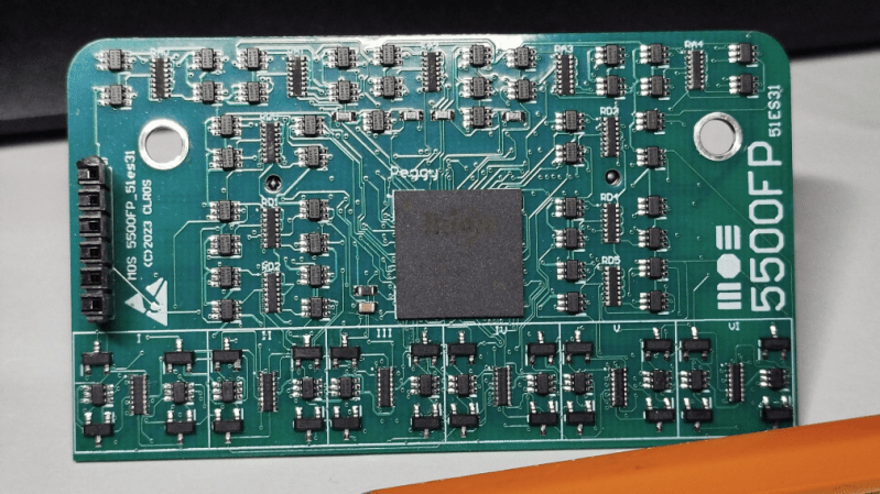
The device in question is called the 5500FP, as outlined in a research paper from [Claudio Lorenzo La Rosa.] Very few ternary processors exist, and little effort has ever been made to fabricate such a device in real silicon. However, [Claudio] explains that it’s entirely possible to implement a ternary logic processor based on RISC principles by using modern FPGA hardware. The impetus to do so is because of the perceived benefits of ternary computing—notably, that with three states, each “trit” can store more information than regular old binary “bits.” Beyond that, the use of a “balanced ternary” system, based on logical values of -1, 0 , and 1, allows storing both negative and positive numbers without a wasted sign bit, and allows numbers to be negated trivially simply by inverting all trits together.
The research paper does a good job of outlining the basis of this method of computing, as well as the mode of operation of the 5500FP processor. For now, it’s a 24-trit device operating at a frequency of 20MHz, but the hope is that in future it would be possible to move to custom silicon to improve performance and capability. The hope is that further development of ternary computing hardware could lead to parts capable of higher information density and lower power consumption, both highly useful in this day and age where improvements to conventional processor designs are ever hard to find.
Head over to the Ternary Computing website if you’re intrigued by the Ways of Three and want to learn more. We perhaps don’t expect ternary computing to take over any time soon, given the Soviets didn’t get far with it in the 1950s. Still, the concept exists and is fun to contemplate if you like the mental challenge. Maybe you can even start a rumor that the next iPhone is using an all-ternary processor and spread it across a few tech blogs before the week is out. Let us know how you get on.


Perhaps interesting for investigating CPT symmetry.
Personally, I’m waiting for the triumphal return of bi-quinary representation of decimal digits.
Tritcoin is my next investment
Ohh, I didn’t realize that Tritcoin ($TRIT) is already on market.
Tritcoin ($TRIT) is a Solana-based cryptocurrency developed by Fractal Tech Corp that uses ternary-based (base-3) cryptography for quantum-secure transactions
. Founded by the pseudonym “Tritoshi Fractalmoto,” it focuses on high-security, privacy-preserving smart contracts, and encrypted audio NFTs.
binary… ternary… next step analog computing (which isn’t all that silly if you want to make a pattern matching machine that requires many multiplications)
+1 for analog. I’d like to see a new iPhone which mimics the human brain with analog silicon and memristors for the synapses.
what a strange thing to say
As a stepping stone to complex analog computing, I’d settle for someone cracking the nut on true asynchronous computing.
I should clarify: I should have said asynchronous processing. Asynchronous computing is the boring multi-threaded high-level coding stuff we all know and love.
Asynchronous processing is deeper, right into the silicon architecture. It uses no global clock. Computation does not go in lockstep and is generally not deterministic in time. It is truly event-driven, and all communications involve a handshake.
As each computational block operates at its own best speed, the approach maximizes performance and minimizes power consumption, though at the cost of increasing the complexity of programming.
Popular a decade or two ago, interest seems to have waned.
https://en.wikipedia.org/wiki/Asynchronous_system
I’ve read about asynch processing in the 1980s no less. The idea was it is handled at the hardware level and everything above that is sugar candy, ie GUI, etc.
Would be fancy to see all three converge, asynch processing, ternary and analog computing. Somehow I see the three are dis-associated with each other, but shouldn’t really be.
Next up, I’m going to create Babbage’s Indifference Engine.
Cat. It’s a cat.
Could this be combined with quantum computing? Qutrit?
Yes, it’s called a quit.
😖
I like trits.
Is this the same guy that got torn apart on Reddit?
It’s worth pointing out that this device is simulating ternary logic with binary logic — FPGA hardware signals can be either on or off, and don’t support the three-state signalling required for true ternary logic, meaning that each trit is represented as two bits. These are then converted via analogue circuitry into balanced ternary for the external bus interface.
It looks like the CPU is written in VHDL, which makes me wonder whether there’s any reasonable code path from the VHDL design to real ternary silicon — I suspect not, meaning they’ll have to reimplement it from scratch with custom ternary tooling. (Which in turn makes me wonder why they chose to do the CPU prototype on an FPGA rather than just emulating it with a cheap ARM or something.)
(Source: the linked paper.)
Thank you for putting in the time to clarify, I was vaguely wondering if this was some kind of new FPGA that could work with 3 voltage levels, thought probably not, and not wanting to be a click-bait victim yet again, didn’t bother reading further!
Simply because, as you have already said, the path to get to an ASIC has already been partially done by writing the circuit in VHDL. The basis is the same: once you have VHDL, you can implement it on an FPGA (using the FPGA provider’s basic cells) or on an ASIC (using the manufacturing process’s basic cells or creating new ones).
If I had used an ARM, it would have been EMULATION or SIMULATION; I would have used an existing CPU to emulate or simulate something else. In this case, we IMPLEMENTED a circuit with FPGA technology. The same VHDL (or with minimal modifications to adapt it to a ternary Verilog) is needed to create an ASIC (but we currently lack the funding, and that’s not the scope of our work).
‘Emulation’ or ‘Simulation’ definitely seem like better descriptors for this than ‘implemented’ since it’s not as if the FPGA configured itself to be a physically trinary device; it configured itself to have the same results as a trinary computer, so the correct outputs appeared on the bus, which is much closer to emulation than implementation.
The 5500FP on the FPGA is an implementation—the RTL directly describes the datapath, control unit, register file, and everything else in ternary logic mapped to binary LUTs.
There’s no interpreter: each clock cycle executes the ternary instruction structurally, not by simulation.
If, however, I had written a C program that reads ternary opcodes and simulates the processor’s behavior on a conventional host, that would be an emulator.
If you have a bunch of discrete components and I asked you to build an AND gate on a breadboard, would that be implementation or emulation? What if I asked you to build a ternary AND gate with the same components?
See, you’re using the same components to structurally build the gate. It doesn’t matter if the components are actually analog and you’re running them in cutoff/saturation mode; no one cares; they care about what comes out as output. You’re implementing circuits that perform specific functions.
The situation is different when you want to create an emulation; you have a system already up and running and you tell it to behave, step by step (with a SEQUENCE of instructions) so that the output is the desired one. In this case, you emulate the behavior of the circuit, without building one.
No, that doesn’t follow. You may be describing the hardware properly as a ternary system in Verilog or whatever, but when it gets to the FPGA it’s not an actual ternary processor.
The FPGA receives information for how to ACT like a ternary processor and EMULATE the ternary processor you described.
An FPGA doesn’t literally connect hardware to physically create the logic gates described. It loads data into a LUT for what the outputs should be for various inputs.
If I had a 2-bit piece of memory with 1 loaded in the 11 space, it would emulate an AND gate but it wouldn’t ‘be’ or ‘implement’ an AND gate.
“whether there’s any reasonable code path from the VHDL design to real ternary silicon”
Unless you write the VHDL at gate level only, it’s the same problem with binary. You might write “a = b + c” in the HDL, but the synthesis tool for the FPGA will map that to the FPGA’s adder structure whereas synthesis for an ASIC will map it to its own (or to basic gates). Same thing with, say, muxes or memory.
No matter what they’re going to need a custom VHDL->ASIC synthesis engine anyway, so if, for instance, you go ahead and use VHDL typing to just pass trits around and then at the necessary level you decode the trit into a binary pair and operate as needed, you just swap out everything past that point with your custom library.
“Which in turn makes me wonder why they chose to do the CPU prototype on an FPGA”
Internally the FPGA is binary, but if you read the paper, the external world is balanced ternary (-V/0/+V). That’s why it’s as slow as it is – the external interface conversion (balanced ternary to 2 bits) is slow. In other words, the FPGA is capable of interacting with actual external silicon operating in balanced ternary.
“No matter what they’re going to need a custom VHDL->ASIC synthesis engine anyway, so if, for instance, you go ahead and use VHDL typing to just pass trits around and then at the necessary level you decode the trit into a binary pair and operate as needed, you just swap out everything past that point with your custom library.”
Yes, that’s exactly how it is. But they already exist and some are also freely usable and downloadable. Try searching for “Triton TPU” on GitHUB.
“That’s why it’s as slow as it is – the external interface conversion (balanced ternary to 2 bits) is slow”
It’s not actually the conversion itself (which is almost instantaneous), but the fact that the external discrete components, in this implementation, don’t support more than 20/25 MHz.
I’m curious how much advantage you’d need to derive from the architectural difference to be able to make up for the implementation disadvantages. The flash memory outfits will do up to 16 distinct voltage levels per cell for the sake of density(since that gives you enough to map all possible 4 bit sequences to a voltage level); but QLC is appreciated pretty much only as the density/value option; and with dense logic ICs the voltage you run them at has a fairly massive effect on power draw, so you’d presumably either need significantly better fabrication or to eat a fairly stiff power penalty to ensure that 3 states are reliably distinguishable rather than just two.
“Maybe you can even start a rumor that the next iPhone is using an all-ternary processor and spread it across a few tech blogs before the week is out. Let us know how you get on.”
It sounds like the makings of an April 1st post…
“the next iPhone is using an all-ternary processor” So say we all.
This is a good place to start: We know that HaD has some kind of high-speed pipe into Google’s pagerank or search algorithms. Maybe this will seed the AI engines as well.
We already use three state logic! Almost every computer bus is tristate: 0, 1 and Hi-Z.
HI-Z cannot be used to represent information; it is primarily used to free up common buses for use by other devices.
We also have HI-Z, but it’s certainly not used as a fourth state!
Didn’t Star Trek say their computers were ternary? The Voyager episode Future’s End, Ensign Kim has to “adapt to the binary system” used in a 1996 computer.
Why is MOS printed on the board?
This is the old logo that referenced “MOS Technology”:
We now have our own logo that you’d like to see on our website.
Damn, “Ternary” before GTA 6