Glass-based substrates are slowly beginning to push out organic substrates – as also commonly used in PCBs – due to often superior material properties for packaging. One area where glass substrates have however struggled is with through-hole vias and providing the conductive copper path through them. A 2024 article by [Keith Best] gives a good overview of the topic, with recent news showing how much companies like Intel are pushing for glass substrates, specifically for the packaging of dies.
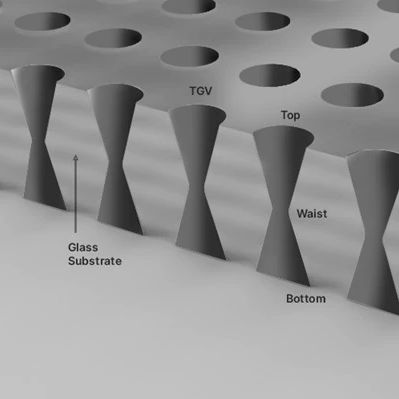
One major advantage with vias in glass substrates is that they can be much smaller, enabling smaller than 0.1 mm diameter holes with far finer pitch. The challenge here is to make perfect holes with a laser that are defect-free, as well as have the intended diameter.
After that this through-glass via (TGV) has to be coated or filled with copper, much like their organic equivalent. Said TGV can be fully filled with copper, or use plating and add dielectric filler. Detecting flaws in such a finished TGV is important.
In a 2025 review article of glass substrate technologies by [Pratik Nimbalkar] et al. published in Chips the state of the art at the time was covered. The need for ever higher-density integration options with ASICs is highlight here, especially now that many chips today consist of multiple interconnected dies inside a single package.
The complications of creating TGVs with femtosecond laser pulses in Borofloat 33 glass are highlighted by [Daniel Franz] et al. in a 2025 research article, with microcracks and backside ablation observed without proper precautions, something which previously was often resolved by an etching step following said laser drilling. The main issue here is the post-drilling residual stress from the thermal shock, which the authors demonstrate can be largely prevented with careful tweaking of the laser drilling parameters.
As pointed out in a 2024 review article by [Chen Yu] et al. glass substrates are useful for far more than just high-density chip packaging. Glass substrates are also chemically resistant, have a higher heat resistance, are largely transparent to RF and can be hermetically sealed against outside influences. This makes them great for various advanced sensors and communication devices.
Meanwhile, if you wanted to do some metal-depositing on glass at home, we covered this recently.


i wonder what thermal expansion difference between a glass carrier and the main pcb will do with the durability. and the thermal conductivity of glass is lower than fr4.
Read the text in the first picture of this article
Glass has much higher thermal conductivity than FR4.
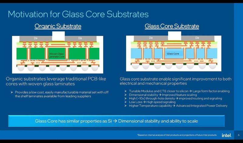
I’m fairly confident the main use for this would be large BGA packages or, even more importantly, their package-less cousins the flip-chip ICs. Instead of using bond wires and attaching those to pars in an IC package, you flip the chip over and press the silicon directly onto the PCB. (Get it?) This saves money mostly because making bond wires is hard and also because packaging is mildly difficult (extra material, gotta make the pins or balls, gotta keep them dry so they don’t pop). The biggest use case for a substrate (PCB material) with a coefficient of thermal expansion that matches silicon ICs is putting many of these flip-chip ICs on a board and allowing them to talk to one another. Don’t let anyone fool you, those glass-substrate boards will then be connected to a normal fiberglass PCB. This glass substrate is intended for very high speed digital/analog/RF applications including ASICs and modern CPU designs. The closer together you can put these devices, the faster they can run. The less the difference in coefficient of thermal expansion, the hotter they can run. Putting all your fancy chips for a laptop (for example) on a glass substrate that runs at 120C (pulled out of nowhere) would allow better performance without burning the motherboard as much as it currently does. Feel free to correct or comment.
Some context hint somewhere at the start would be helpful. We are talking Chip creation?
I’m sure there’s a Start Trek scene about out-of-context jargon somewhere.
I guess so.
When looking at the first picture, there is a “die” in top, and on the bottom something that looks like BGA bumps. That would put it in the application area of an interposer. https://en.wikipedia.org/wiki/Interposer
And then there is also an overlap with LTCC (Low Temperature Cofired Ceramics), which is 3D printing for interposers, which then get fired in a kiln.
yeah i still haven’t figured it out. Is this about PCBs, and the traditional ‘fiberglass’ is being called ‘organic’ because the resin is a carbon chain polymer? Switching to solid glass seems wild but i guess i’ll believe it when i see it
Apart from high-density silicon IC packaging, it’s very good for RF applications.
https://www.3dgsinc.com/rf-sip
https://blog.samtec.com/post/should-i-design-on-glass-top-5-things-to-know-about-gct/
Any chance this is meant to be a glass ceramic for low thermal expansion?
Just wondering… if I would like to use Windows would a glass substrate CPU be better suited? And If I wanted to use Linux (you know, the OS with the penguin mascot) would a substrate based on ice be better for that? And for those wanting to use MacOS (you know, the OS with the fruity logo), a biological substrate perhaps.
Then there are ceramic substrates as used in IBM’s Thermal Conduction Module. Many-layered, with shrinkage during firing controlled better than anyone had believed possible so chips could be mounted on solder balls direct to the substrate (“flip chip” ). Traces on each layer were printed in molybdenum paste, which sintered with the ceramic at the firing temperature; I don’t remember whether vias were just printed and melted thru or if something more was done.
Of course extracting heat when the active face of a bipolar chip was against the ceramic was a challenge, which is what the rest of the TCM did. (Spring plungers and helium, water cooling packs.)
Seconded.
I have a whole archive of HP Journals, Analogue Dialogue, and other technical articles from the 1950s through the 1980s when ceramic substrates were the new/hot technology. Then apparently someone watched The Graduate and the one word for the future becane ‘plastics’.
This smells like a corporate “oh crap, everyday people can get PCBs made at a reasonable price these days, so we’ve lost our ability to leverage capital investment for market advantage. Quick, go invent something ordinary mortals have no hope of doing on their own. We’ll call it a new paradigm and dodge any questions about how this is measurably better in any real application.”
Might be easier to make at home as well.
Wait, 0.1 mm holes? You can fit an entire smartphone SOC through that these days.
Huawei is now talking 1.4nm tech, think about it, 0.1 mm is gigantic.
TSVs are 3-4 orders of magnitude larger than transistor featues.
https://www.emworks.com/application/how-does-through-silicon-via-tsv-enhance-chip-performance-and-efficiency
https://semiengineering.com/whats-next-for-tsvs/
“The size of the TSVs vary depending on the application, from tens to hundreds of micrometers for CMOS image sensors, tens of micrometers for silicon interposers, and sub-5nm for backside power delivery.”
A micrometer is 0.001 mm, and a nm a thousands of that.
So 0.1 mm might be a limiting factor from glass vias here? Might force compromises if you use glass I would think. But I suppose it’s always a balance with any material, since a perfect one across the board is unlikely.
And as they develop trick to make them as small as possible we might find new uses for the same technology.
I imagine the ability to make tiny holes in glass would enable new things outside classic chip manufacturing. I just hope it won’t be military stuff, or stuff to degrade privacy and personal freedom.