The radio frequency world is full of mysteries, some of which seem to take a lifetime to master. And even then, it seems like there’s always something more to learn, and some new subtlety that can turn a good design on paper into a nightmare of unwanted interference and unexpected consequences in the real world.
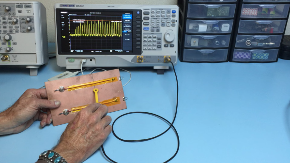
As [Ken Wyatt] aptly demonstrates in the video below, where you put gaps in return paths on a PCB is one way to really screw things up. His demo system is simple: a pair of insulated wires running from the center pins on BNC jacks and running along the surface of a piece of copper-clad board to simulate a PCB trace. The end of each wire is connected to the board’s ground plane through a 50 ohm resistor, with one wire running over a narrow slot cut into the board. A harmonics-rich signal is fed into each trace while an H-field EMC probe connected to a spectrum analyzer is run along the length of the trace.
With the trace running over the solid ground plane, the harmonics are plentiful, as expected, but they fall off very quickly away from the trace. But over on the trace with the gapped return trace it’s a far different story. The harmonics are still there, but they’re about 5 dBmV higher in the vicinity of the gap. [Ken] also uses the probe to show just how far from the signal trace the return path extends to get around the gap. And even worse, the gap makes it so that harmonics are detectable on the unpowered trace. He also uses a current probe to show how common-mode current will radiate from a long conductor attached to the backplane, and that it’s about 20 dB higher with the gapped trace.
Hats off to [Ken] for this simple explanation and vivid reminder to watch return paths on clock traces and other high-frequency signals. Need an EMC probe to check your work? A bit of rigid coax and an SDR are all you need. Continue reading “The Perils Of Return Path Gaps”


