Preferring to spend hours typing code instead of graphically pushing traces around in a PCB layout tool, [James Bowman] over at ExCamera Labs has developed CuFlow, a method for routing PCBs in Python. Whether or not you’re on-board with the concept, you have to admit the results look pretty good.
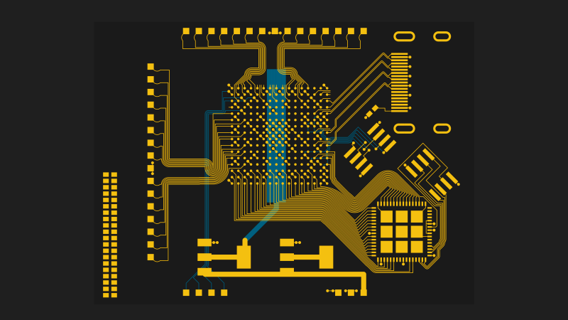
Key to this project is a concept [James] calls rivers — the Dazzler board shown above contains only eight of them. Connections get to their destination by taking one or more of these rivers which can be split, joined, and merged along the way as needed in a very Pythonic manner. River navigation is performed using Turtle graphics-like commands such as left(90) and the appropriately named shimmy(d)that aligns two displaced rivers. He also makes extensive use of pin / gate swapping to make the routing smoother, and there’s a nifty shuffler feature which arbitrarily reorders signals in a crossbar manner. Routing to complex packages, like the BGA shown, is made easier by embedding signal escapes for each part’s library definition.
We completely agree with [James]’s frustration with so many schematics these days being nothing more than a visual net lists, not representing the logical flow and function of the design at all. However, CuFlow further obfuscates the interconnections by burying them deep inside the wire connection details. Perhaps, if CuFlow were melded with something like the SKiDL Python schematic description language, the concept would gain more traction?
That said, we like the concept and routing methodologies he has implemented in CuFlow. Check it out yourself by visiting the GitHub repository, where he writes in more detail about his motivation and various techniques. You may remember [James] two of his embedded systems development tools that we covered back in 2018 — the SPI Driver and the I2C driver.


I have to say, I like the concept. I make an analogy with the mechanical design world where I have embraced OpenSCAD. I would much rather write code that click away on some GUI CAD system. This promises to be the same kind of thing for PCB layout, which sounds great. Keep at it!!
Every major commercial mechanical CAD package supports both GUI and Code based development of models, openscad is not unique in its approach to modeling through code.
Some of us can be far more productive CAD wise not writing code and all major packages support parameterization, so the ‘coding’ is still there. If you are a programmer, everything is a program. Many in the CAD world have a more artistic drawing entry into it. Whatever works.
It looks nice, but I highly doubt the end result would hold up for high-speed designs using a BGA like that without a lot more concern for design rules and simulation. It doesn’t even look like this tool does length matching, nevermind impedance or transmission line resistors.
i really want a scripting language that defines schematics. i have made several false starts but i haven’t come at an abstraction that seems useful. what i want to avoid is doing a whole bunch of manual touch-up each time i insert something in the middle, because then i feel like i might as well be drawing schematics in ascii art (which is how i generally do it today).
i don’t expect (or really desire) entirely automatic routing from a netlist or whatever, but i also want to be able to easily shift two networks apart to add a component between them, without re-visiting too much. i’m certain there’s a good way, but i haven’t found it. some way of specifying the circuit such that there is a naive layout engine that makes the simple choices by default (like putting series components in a straight line with eachother), but can be overridden on details (whether that line is horiz or vert, or with an elbow in the middle, for example). i just haven’t had the idea yet, i haven’t figured out how to do it any better than like SVG with a component library, where you have to update a bunch of coordinates any time you insert something new.
While intended for ASICs, the various HDL languages (verilog, VHDL, etc) were intended as an alternative to designing the logic schematic as a pictorial representation (they just also happened to allow ‘primitives’ – logic gates – as part of the native language but there’s nothing to stop a user from using explicitly instantiated modules and only having wires between them).
If you go even further into the ASIC design world, there are methods that allow additional meta data to be associated with modules (IPXACT springs to mind – it’s used by Xilinx’s Vivado tool with their packaged IP). Equally, it’s possible to embed location data within the files (VHDL has the ability to just insert ‘string’ properties of which tools can then interpret the data in meaningful ways, such as forcing pin LOCation).
While HDL may seem like the reserve of just “things within an ASIC”, they can be used to describe multiple chips wired together externally, after all, a lot of what now lives within an ASIC used to exist as multiple (external) devices.
There are several layout programs that do something very similar to what you’re asking, Altium and Xpedition. The problem, or trade off, I’ve experienced, is that in designs where this works, the amount of time it takes to setup the rules and constraints is similar to the amount of time it takes to manually route. Furthermore, most designs I’ve worked on, benefit very little with auto routing.
It works well with basic designs, such as interface boards. When you get into more complex designs, you have more constraints and more to consider. The pieces of software that can handle these designs (Xpedition) already has these auto routing features that will take care of the ‘easy’ routing or has features that help enough with routing that requires tuning, length matching, etc… and so it really does not seem to add any big time saving on complex designs.
For relatively simple designs and for people who aren’t backed by companies with tens of thousands of dollars to buy that software, this looks promising!
Wow, awesome work.
For me, Schematic entry for electronic design over textual any day .
However, I cannot stand graphical programming like labview.
This is a preference thing I think. ? Or is it?
Is this consensus reversed for those who prefer textual schematic design?
Question: Are there people who have difficulty using their eyes / visual cortex for imagining a system/solution from symbols other than text?
There is a deficiency where those neuro atypical do not have a “mind’s eye”. They cannot imagine a red apple. They can recall stuff they know about a red apple, but no internal image forms from it. Interestingly enough, they also have difficulty getting scared from scary stories.
Having a “mind’s eye” is linked to being a reader during your development. *Most* (but not all) people who are observed not having the ability to visualize in their mind also did not read much in their formative years. They also tend to not have great language skills as it appears that reading develops the centers of our brains that are responsible for spoken language.
Then you have the particularly neuro atypical like me. I don’t have a “minds eye”, but I can manipulate complex geometries in my head without actually “seeing” them in my mind. I have been an avid devourer of books since I was a young child, but I have mild issues with processing verbal communication. I’m also virtually blind to non-verbal social cues from people I’m not close to. I manage to muck my way through the world, but I’d have a lot easier time if “normal” people would clearly communicate and stop with the needless vagary….
Welcome to the wonderful world of the autism spectrum :/
Citation required. Does not apply to me, nor to my son. We both read a lot, and have good language skills.
It’s called congenital aphantasia and has received renewed interest of the scientific world in the last few years. It’s also a real bummer to have. I couldn’t imagine or describe my wifes face if my life depended on it. The weird thing (and plenty of people have the same story) is that I didn’t realize that it was something that I couldn’t do but other could until I was about 25. Really weird.
Most people suck at describing people’s faces, that’s really nothing uncommon.
Recognizing and seeing them is not the same.
Seeing them in your mind*
Schematic entry works well for a lot of PCB projects, but for some type of projects it just does not make much sense (But is used anyway by lack of alternatives) When you work with FPGA’s or other 1000+ pin parts then a schematic just looks likes endless lists of pins connected to labels.
SKiDL (mentioned above) seems a better fit for such projects. Generate those 100+ decoupling caps in a for loop. Use lists to connect databusses. Use a script to extract pin names from your FPGA tools. Use a loop to generate arrays of multiplexed or charlieplexed LED’s.
for me, i prefer to look at a schematic. i very much like the visual diagram. it’s just the entry and change-tracking that i’d rather do by text. i don’t like the UI of any of the schematic entry programs i’ve used, it might as well be MS Paint or XFig so far as i care. and i hate having inscrutable changelogs, where you feel like you’re lucky to get massive XML full of irrelevant metadata you don’t care about instead of an atomic binary blob.
Some of the ideas here are very cool! I still prefer graphical tools for PCB layout, but it would be great if KiCAD would eventually get a feature where you could define a river for a set of signals, and it could be regenerated automatically when needed. Kind of like how zone fills work, you draw the general line and it would route all the signals around obstacles, and if you later need to move some other parts, just clear and regenerate.
This is sometimes called “guided routing”. You take a bunch of signals (for example a databus) assign it some board space or a general path and then your PCB program fills in the details.
Using that as search term for youtube finds a video from Mentor / pads and they calls it “Sketch routing” https://www.youtube.com/watch?v=Yn32jdFlUcQ
Altium has something similar too for the last few releases. The “ActiveRoute” Feature. It works pretty well, but not as well as the sketch router in Xpedition.
It certainly looks impressive, and I’ve always considered schematics a relic of the past for boards that are mostly comprised of digital interfaces.
However, I always thought that running signals in parallel is something you avoid as much as possible in PCB layout, and here it’s done in places where it’s clearly not required. Of course, whether that’s an actual problem depends on the signals.
Neat. This has a very interesting potential for parametric routing, where for example one has a defined schematics declined in many PCB variants.
That sounds cool. I would love a parametric PCB to support different USB connectors.
What we need is someone from the photoshop UX team to look at the KICAD UX.
UX is still the place open source suffers most.
I should be able to sketch out a schematic as quickly as I can sketch in photoshop.
And I shouldn’t be the one wiggling parts back and forth to make them align!!
What are all those antenna on the PCB ?
Bwaha, my thought was more “oh dear lord the crosstalk.”
Really, the most useful thing here to me is automatic pin/gate swapping, except for me the basic concept of swappability at the pin/gate level is *way* too simplistic. MCUs don’t all have total pin crossbars, and FPGAs have lots of functional pin groupings (DDR byte groups, banks, analog inputs, differential pairs, transceivers) at this point. And even with FPGAs you might *think* that two adjacent pins are identical, but if they’re *actually* bonded to two distant portions of the chip the propagation delay might be huge.
Could you imagine if instead of specifying identical gates and identical pins you could just specify resources and constraints that certain groups provide and allow it to connect up the resources in such a way as to make the routing totally trivial? I mean, with FPGAs/CPLDs if you could integrate it with route delay estimations and such, that would solve *sooo* many problems.
That board looks like it has no decoupling capacitors all, or if it does, they’re far away from the ICs with long, high impedance loop paths.
There doesn’t appear to be any groundplane.
Any accommodation of length matching, differential pairs and impedance control?
This approach seems to treat the layout as a set of ICs and connectors that are connected together with a matrix of “ideal wires”, and we don’t care about the placement, layout, thickness, crosstalk, impedance, length, prop delay, current capacity and resistance of those wires – they’re just assumed to be perfect ideal wires that don’t really exist.
When I looked at the PCB I also noticed similar things (but not everything you mentioned) as well as traces routed at right angles, which of I remember correctly is a basic no-no of routing.
Seems like it might be fine for simple TTL circuits, but maybe it needs a well-experienced PCB designer to help with the routing rules and design constraints?
A good and promising start and still a long way to go: routing with rivers and crossbars have a lot of potential for automation without a need for too much human attention, but on the other hand rivers appear to be at odds with high speed design requirements (and cross bars would break ground plane return paths too harshly). Probably some combined approach is possible, using different routing methods for low speed “rivers” and for high speed diff pairs. I believe one day we’ll have a HDL toolchain with a fully automated placement and routing for PCBs. It’s much harder than for ASICs, but still possible.
This really is something clever in such a short form. Basically you have a way to script/compile a PCB to the point of manufacture in one command. Its like saying synthesise me a PCB. Its also a way of producing a PCB for someone who has never produced a PCB. I think you will have to put the signal integrity issues aside until this routing schemes for this getting better Or more definable. It really is elegant..
But for those of you who want to script or compile a schematic to a PCB its much harder when you do it for real. Many years ago i produced a process for synthesis of schematics from HDL script. The board itself we made was an MCM module (old i know) who’s interconnect and operation was already defined and simulated in HDL. The HDL held the interconnect of 4 chips. We took the HDL and then synthesised this into a schematic. The tool was Mentor Graphics scm ( old schematic Falcon Framework synth tool). We now had a large flat multiple sheet schematic of the MCM but now needed to hook it up to real PCB IC package footprints and the rest of design.
Using the Mentor Graphics hierarchal levels we went down a level to hook the HDL synth schematic to real PCB foot prints. This produced another layer of schematics. We then went up a level to hook the HDL synth schematic to all the ancillary parts of the PCB i.e. voltage regulation, decoupling , Analog sections, Clock section, Connectors etc… . This completed the schematic design. NOW for the problems…Everytime you changed the HDL (small mods) the whole synthesised schematic became an un-recognisable drawing from the previous synthesised schematic. It then required work to re-hook down to the PCB package footprints and work to hook back up to the the higher levels. So unless you have a huge interconnect ( ie > 20 Asics/FPGA) to hook up the benefits were unclear. You also need a well governed schematic entry process and PCB flow to match. The MCM schematic was then taken to PCB layout and produced more traditionally some balance of Manual route and Auto route with timing constraints and signal integrity constaints. We entered the integrity rules via a script.
So we learnt a lot about PCB flow problems to make this work well. But you really need to look at defining a whole Design flow end to end and some good engineers who can except a change from more traditional flows – not easy!!. It really only becomes beneficial for large interconnects where like someone said earlier in the comments “endless lists of pins connected to labels” — SO True!!. So you might benefit more from some tables entries to drive the schematic. Something like “import interconnect” tables from a CSV spreadsheet file and reproduce this on the schematic. That way you keep the schematic floor plan relatively static but drive the large interconnect by easier methods than drawing.
I also did something like this for large connector schematics to be driven by an imported table. It really only produced a schematic of wires with net names to connector pins but something like this in Kicad could be beneficial. Hardware engineers also like working in spreadsheets to defining pin outs. Its more visual.
So i hope this helps someone…