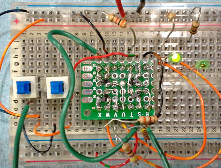
[Fran] went all-out with her reverse engineering of the Apollo Saturn V LVDC board. Regular readers will remember that she was showing of the relic early this year when she took the board to her Dentist’s office to X-ray the circuit design. Since then she’s been hard at work trying to figure out how the thing functions using that look inside the board and components. When we say ‘hard at work’ we really mean it. Not only did she explore many different theories that resulted in dead ends, she also built her own version of the circuits to make sure they performed as she theorized. Above you can see her version of the NAND/AND gates used on the hardware.
We find her explanation of how the logic devices were originally fabricated to be very interesting. They started with a ceramic substrate and used additive processes to form the traces and add the gates. We’ve embedded her video explanation after the jump.


I wish I had that kind of determination…
I’m a windows user, so often enough I’m forced to have it :/
I see lots of automotive modules made in the 70’s and 80’s that were made using this technique. We have a *lot* to thank the lunar programs for as far as technology advancements.
Wow, what an interesting project. I’m going to have to bookmark this and watch/read it all later. Fascinating.
An excelent example of [and how to] reverse engineer[ing].
These circuits are discreet logic examples of what at the time
became TTL [transistor-transitor Logic {7400 series}]
It’s much earlier than TTL though, more like RTL. In fact this wikipedia article mentions its use in the AGC which I guess was a quite separate part of the same program.
Beautiful work and presentation.
Correct. TTL logic was just becoming available when these great spacecraft were being launched so minor tweaks to the later ones were in fact that kind of circuit design. But all, and I do mean all of them were designed that way. Bitsavers, a site dedicated to saving documentation on everything computer contains some manuals on it, and also some IBM manuals which’re perfect for what the lady is doing…..
IBM simply directed their successes at building the S/370 modules to the ones for the Big Bird, and indeed everyone later, Space Shuttle included.
Yes, the AGC was RTL, but the circuits in this article are clearly TTL, built from individual transistors since they pre-date 54/7400 series chips.
And when I say “hard at work” I really mean it too. Trip to HR for sexual harassment, every time.
http://bitsavers.trailing-edge.com.nyud.net/pdf/ibm/nasa/Saturn_V_LVDC_Vol1_Jan65.pdf
Here is all the info on it from IBM
S/370 is WAAAY too late. S/360 became available in 1964.slrarick@ix.netcomcomStan