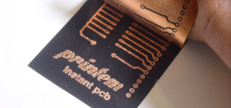
We are going to great lengths to turn a quick idea into an electronic prototype, be it PCB milling, home etching or manufacturing services that ship PCBs around the world. Unwilling to accept the complications of PCB fabrication, computer science student [Varun Perumal Chadalavada] came up with an express solution for PCB prototyping: Printem – a Polaroid-like film for instant-PCBs.
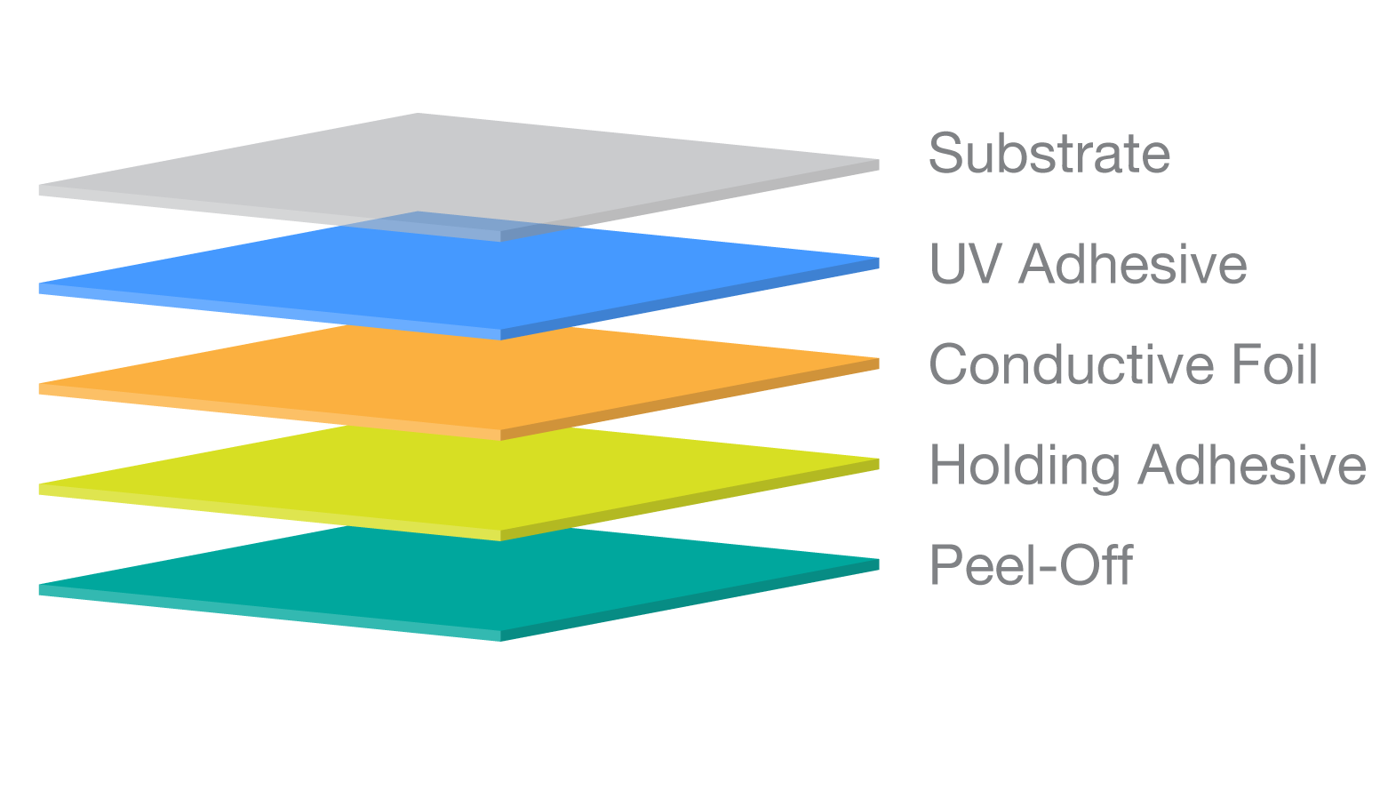 Printem is a photosensitive multi-layer assembly, similar to presensitized copper clad – but with an instant development feature. It consists of a thin conductive copper foil that is held to a transparent carrier substrate by a photocurable adhesive film. The other side of the copper features a layer of holding adhesive and a peel-off back side.
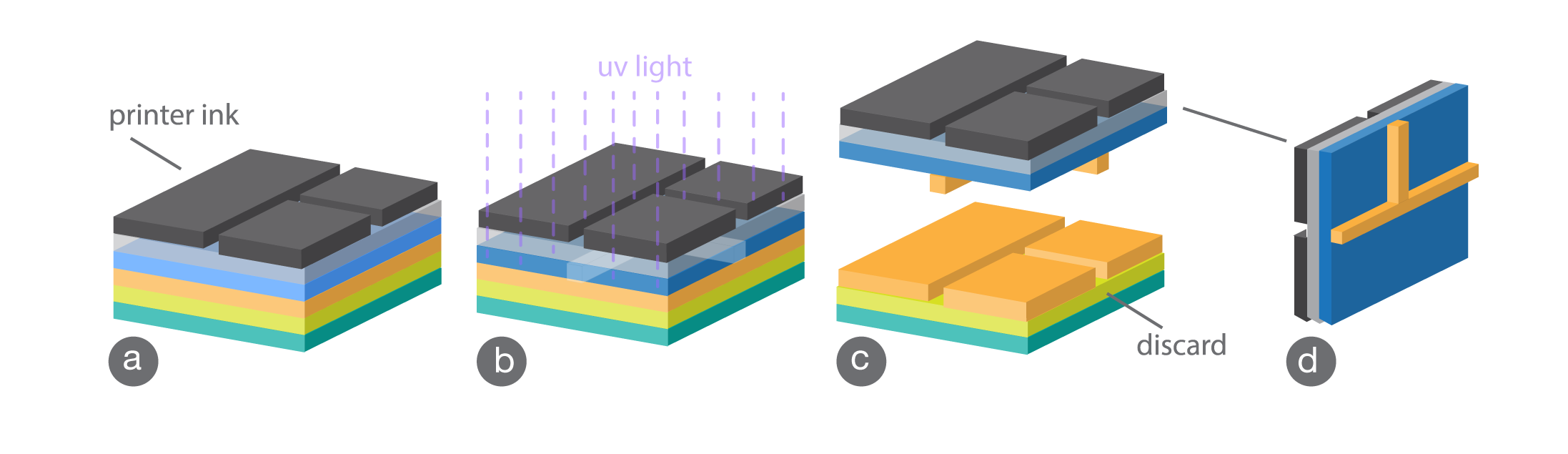
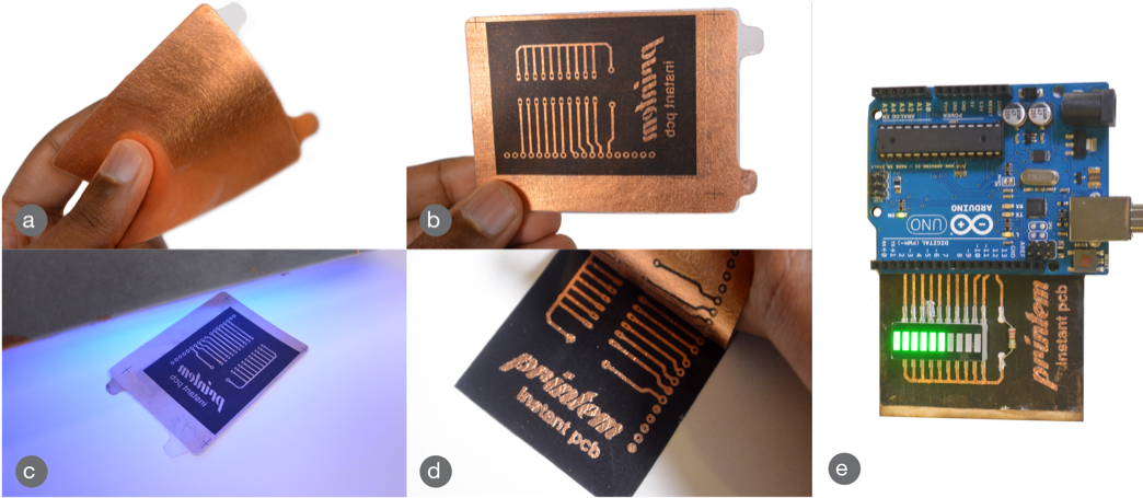
To turn the Printem film into a PCB, a negative of the copper traces is printed onto the transparent substrate with help of a regular inkjet or laser printer (a). The film is then exposed to UV light (b). Where light shines through the printed mask, the photo-adhesive cures and selectively fuses the copper film to the substrate. After exposure, the back-side with the holding adhesive is peeled off (c), taking the un-fused copper-portion with it.
The copper layer is very thin, about 100 times thinner than on regular PCBs, and breaks clean enough around the contours of the exposed regions to form copper traces. The result is a flexible PCB (d) that, depending on the substrate material (acetate or polyimide), can even be soldered at low temperatures. For those who want to learn more about how Printem works, [Varun] has put together an interesting writeup on Hackaday.io.
Printem is a project at the DGP (Dynamic Graphics Project) lab of the University Of Toronto and has been recognized by the University as one of the Inventions of the Year. As co-founder of Printem, Ph.D. Student and busy inventor [Varun] now works on the commercialization of his instant PCBs with support of the University’s accelerator network. Enjoy the explanatory video below and let us know what you think of this in the comments!


Not sure how fine a trace you could print using this method (the demos are noticeably lacking this) but for a quick flexible circuit it’s hard to beat.
FYI comment section: https://hackaday.io/project/13270-printem-instant-printed-circuit-boards
>varunperumal wrote 9 hours ago
>We are working at about 24 mils traces with 24 mil spacing right now, thats probably not very useful for any circuit that is moderately complex. ( Pictures and making instruction soon to be updated )So we are testing several improvements to bring it down to 10mil traces with 10 mil spacing.
This is so much better than that ‘circuit printer’ (Voltera?) it isn’t funny.
Isn’t this basically the same as PCBs on glass? Seems like a lot of accolades for what is essentially just a slight tweak on another idea.
and it has been patented. That’s cool, steal an open source idea and patent it.
IMHO they are quite different.
The mechanism of copper removal differs quite a lot; glass pcb technique uses ferric chloride or some other etchant (chemical removal) while printem uses cured uv glue to literally rip copper away (mechanical removal).
Not to mention that it’s nearly a self contained package and not having to use chemicals or heat is a huge plus because now it’s a process that’s safe enough to use everywhere and for everyone.
While I admit is has been made more user friendly, you neglected to mention that glass pcbs also use uv curing in the process. The removal of unneeded copper may be slightly different, but other than that, it’s the same.
I did not mention it because the UV glue serves two completely different functions for both types of PCB;
The glass PCB uses the UV glue because it does not react to the etchant and has a low viscosity which helps getting the copper film flat. It has not been chosen because it’s cures under UV light, it has been chosen because it’s other properties are very handy. Had there been a different glue with low viscosity and resistance to the etchant then it would not have made a difference whether it would be UV glue or not.
With printem the UV glue has been chosen specifically for it’s UV curing properties because without it the entire mechanism of creating the PCB design would not work.
Simply because two processes share a subset of components does not mean that the processes are the same even if they share a similar outcome.
Have you even bothered to really compare the two or are you just trolling by shouting shit about patents?
No.
Yes.
How much current can these ultra-thin traces take?
Depends on how wide they are and what temperature rise you can tolerate.
Assuming the “100 times thinner” in the article is accurate, using the KiCAD PCB calculator, with a 30 degree Celsius rise, for a 10 mil trace you’re looking at 50 mA and a 0.19 ohms per millimetre, and for a 50 mil trace you’re looking at 164 mA and 0.039 ohms per millimetre. Or with a 70 degree Celsius rise, 74 mA and 238 mA respectively.
For comparison, standard 1 oz copper (0.035 mm) can take slightly more than 28 times the current and would have 1/100 of the resistance.
Thanks for doing the math.
Doesn’t look like this would work well for me, but others here who are experienced with micros might use it.
Still a very interesting technique though.
If the traces have such resistance then circuit calculations become that much harder, you suddenly haw to calculate the resistance of every trace into it. Especially if you aren’t simply lighting up a LED or some such stuff.
Makes the whole thing a bit disappointing and I’ll continue waiting for a real breakthrough.
Interesting. The first question burning thru my head would be how well the adhesive works, especially if you solder components on it (heat!). It could probably hold some small passives well enough, but what about connectors, larger power passives or the LED shown in the picture? Is the copper trace just going to delaminate if you apply a little bit of mechanical stress (vibration, circuit board handling,…)?
The very thin copper thickness probably is not the biggest issue, as you could just add more material to the traces with chemical- or electrodeposition, once you have the basic conductive layout on a carrier board.
If that turns out to be a problem then glue it to the top of the board.
I think this is designed for rapid prototyping rather than long-term use.
If you have to start using chemical or elecrodeposition to make it viable, it loses all purpose. Then it REALLY becomes essentially the same process as glass pcbs.
Um… Maybe I’m easy to impress, but I think this Idea is pure genius! wow…
Am I the only one who thinks people need to rediscover chemistry? It still remains the most viable method to make PCBs at home.
Yes however it is messy, this isn’t. For anyone that makes very few PCBs this should be easier, require less equipment etc.
Until very powerful semiconductor lasers become really cheap (ablative metal removal), wet chemical etching is the best DIY way…
Amen.
What about EDM?
I agree. People say ferric chloride is messy. I’ve done several pcbs this way, and I haven’t found it messy at all. Maybe some people just have butter fingers.
Been there. Done that. Burnt holes in the t-shirt!
Seriously though.. you are correct that home chemical etching IS viable however it’s still a pretty rough process and the hobby would very much benefit from something better.
CNCs are a good way to go if you don’t like chemical etching. You can build a DIY model for very little money.
Chemistry is great if you love trying to dispose of hazardous waste at home…
if you are etching with the right chemicals then you would only have waste every few years or so, unless you are making thousands of etches then the various regenerative chemicals can be reused, most just by bubbling air through them.
Of course you are speaking of Cupric Chloride, which is made using simply HCl (pool cleaning chemical, Hydrochloric Acid) and H202 (Hydrogen Peroxide). After the first PCB is etched, it becomes Cupric Chloride or CuCl. As it is “used up”, you can either add more Hydrogen Peroxide, or simply bubble air through it. The added oxygen combines with the excess copper, renewing the solution.
When you rip the copper layer you don’t get a smooth edge and those protuberances will add unknown amounts of impedance and capacitance.
Another idea: instead of soldering a conductive glue can be used to place the components on the “board”.
“Conductive” glue isn’t as conductive as copper. It’s more like a low value resistor than it is like a wire.
Don’t get me wrong, I’m not really knocking your idea. I’m sure it would work just fine for some circuits. Any application that is so sensitive that you need to be concerned about the little bits of reactance from those ripped edges… I would recommend getting out your soldering iron and trying Manhattan construction.
A concern perhaps if you’re doing GHz level stuff, but for the everyday stuff for which such an idea is intended, not a particularly huge problem.
First of all this is really amazing!
Does anyone know how it compares to 3d printed pcb using something like functionalize f-electric filament (0.75 om/c^3)?
The benefit in 3d printing is that I can create multi layer boards and if I don’t mind the height too much I can create traces that are thin but have some depth so it (correct me if I am wrong) can give me less resistance.
Foil transfer is an old idea, even if combining it with photosensitive adhesives isn’t. However any method like that will have the risk of developing very fine and hard to detect cracks in the tracks that may act in unexpected ways as their edges oxidise and form a conductor-semiconductor-conductor bridge.
True, it’s basically a modification of 150 year old foil stamping techniques with UV cure adhesive instead of heat.
Heyyyy, heat sensitive adhesive, specially made “CD” shaped boards, and lightscribe drives….
Would Bluray and UV adhesive work?
I think that gets you into reengineering the player, because it wants to write packets of data in a defined format at higher RPM, rather than arbitrary graphics and text at low speed.
Try gold leaf pressed under heat onto laser printed Kapton. :-) No UV required and it will conduct better too. Less risk of cracks as pure gold is so malleable, and you can always “tin” it with a silver alloy to make the tracks thicker and to facilitate soldering.
And how is this superior to regular photo PCBs? Just because there is no etching? But it trades that for low current capability and likely shitty reliability. Na, thanks. As open source idea, maybe, as commercial product, no. This is going to either boil on low power in niche markets or just flame out altogether.
Just a friendly reminder, this isn’t EE Times it is HACK a Day. Keep your commercial product flames out of it!
I don’t see what you see here. Where is he flaming commercial products? Saying that he wouldn’t buy it but would be willing to try it were it open source isn’t flaming. It’s stating his opinion on its usefulness/value to him.
This is something that you can get into with a very low initial investment, and no hazardous chemicals to bother with.
With this, if you need one board, you buy one board.
With etching, instructions involve a laminator, and chemicals that you will have to dispose of later, plus a much larger cost up-front.
If you are doing a larger number of boards, etching is probably the way to go. However, for one or two boards, this technique might be a lot more cost-effective, as long as you can live with the limitations.
it isnt going to be more cost effective, etching can be virtually free with reusable chemicals.
in the single cent per board price range in materials.
It always amazes me how people flock to a new process of making PCBs – even if it is 1000 times worse than existing methods.
Ugh. I wanted to like this one, but man those boards look like a pain to use. Is everyone else in that much more of a hurry than me that they can’t go to OSH park?
Over two weeks isn’t exactly timely. By the time it arrives, I just don’t really feel like doing the project anymore.
ink, inkjet printing and uv-light, does not seem very innovative.
wonder if it would be possible to make something, using a thermal printer,
where the heat, is use to develop directly, non-inverted pcbs instead of inverted ones using uv-light.
and by using heat, it would be more usable for soldering and reflow.
no uv light, no ink. instant 57 or 80mm pcb’s – at up to 300mm/s.
maby in 2 versions, thick flexible and thin stickers/lables.
With all the hate we always have for KS in these comments, this is something i want to see on kickstarter, take my damn money!
This remembers me of a dry film 20-30yrs ago:
A mirror-like silvery metal film (probably Al or Ni) between a thick and a thin Mylar film and probably similar glues as here. You had to expose it with UV light and peel the two sheets apart.The result was a thin negative and a thick positive image. I tried even to solder to the traces, which was difficult because of the low melting point of the Mylar carrier. But they were conductive.
There is a lot of valid criticism here, but this product still serves a purpose. Think of it this way – we use breadboards for Alpha-Testing a circuit. This could be used for Beta-Testing a circuit board before it goes to a more permanent and properly etched circuit board.
Depending on precision ( can it do thin traces, like those for a TSOP48 flash chip ) . Can it withstand soldering ( if it is marketed to inexperienced people, art people, people without soldering experience, it will probably be handled somewhat roughly ) .
Possibly, with the right choice of adesive, the traces can be bonded very resistantly to the board.
And also price. If it costs a lot more than the chemical way, well, then it turns to something of use in limited situations. But hey, for a quick prototype or temporary repair somewhere without better resources, it could be useful.
Get some copper chloride and copper plate the traces thicker? Considering what I assume are the limitations of trace with/separations I think I’ll just stick to milling boards (not knocking the idea. The more ideas out there, the more likely one will inspire a really good idea).
What’s your setup? We’ve got a CNC in our hackerspace but we’ve had limited success with milling PCBs because they’re not flat enough. A vacuum table would probably help?
The best way to deal with that is probably to probe your board height at different locations before starting the milling process and compensate in software. Basically the same procedure more and more 3D printers use for uneven/unleveled print bed compensation (there are open source solutions you could use as inspiration).
Some machines use the copper board and milling tools directly to make a simple electrical probe, if the tool touches the copper you close a conductive path thru the tool and sample the z-height at that event. Of course, there are other ways to make a z-probe too, again, you can look at the 3D printing comunity for inspiration. I would advise to go for a high precision solution, since you are trying to mill away not much more than 35µm of copper.
Wow, so many people griping about this!
Seriously, folks, this is a rapid prototyping aid, not a long term solution. It’s the next step beyond breadboards. If anything, it gives one a chance to see if their PCB layout will work PRIOR TO sending it off to a board house and waiting 2 weeks for your boards to come back.
Please stop lambasting this for what it isn’t, and take a good look at what it actually is. It may be a new take on an old idea, but it is unique and useful. I, for one, am very impressed.
I have absolutely no problem with taking public domain/open source ideas and improving upon them in an open source way. I don’t like that this idea (at least to me) seems like it’s patenting processes that were in place before they got combined in an incremental way. It’s no more or less impressive to me than glass pcbs or plastic film pcbs, because it’s basically the same thing.
Valid criticism is not “griping about this”.
If your circuit can tolerate the reduced conductivity of this very thin copper, then how about laser cutting thicker nickel foil (it works—I’ve tried it) glued to a laser-resistant substrate? I’ve been thinking ceramic, but there are probably lighter, sturdier alternatives. (Suggestions? I’ve tried glass, but it almost always cracks.)
If you look closely, the printed PCB is somehow attached to a bit of wood before being soldered to the Arduino.
I wonder if something could be done en-post to this project to increase conductivity? Could the board be tinned? Would that destroy the substrate? Can the board survive a low-temp reflow (i.e. busmuth) or would we be stuck with conductive inks?
Jumper wires!
Hi, I am one of the co-creator of this project. We are experimenting with using thicker ( not as thick as traditional PCBs ) but more than simple “leaf foils”. Additionally we are experimenting with allows of cooper and gold that increase the conductivity as well as the malleability. We have made samples that can be soldered using a low temp bismuth solder ( will post pictures and results on the project page in the coming weeks )
The next version that we are making uses much more resilient substrates and adhesives. It should support reflow under 250C , although its not confirmed since we are still testing it out.
Btw, I am a huge fan of your ESP8266 Analog TV project, its awesome !!!
That would be really cool. The only thing I am left thinking is maybe it would be easier to use another chemical to go back and improve conductivity, whether it be actually tinning the boards, or using something like liquid tin to do a deposit.
As always <3 the low-temp solder paste… Solder paste is really the only way to go. So many people have tried to find ways around it, but if you need to do a QFN or similar chip… Solder paste.
Thanks! I am surprised that that was the one you selected for being a fan of.
P.S. Your goal should be to get an esp8285 running on your PCB tech. I know it's a ways away (0.5mm bsc and all) but, there's only 6 external components needed.
Hi, my name is Varun, I am the co-creator of Printem. Its been very encouraging to see all the interest, support and critique of our work. I just wanted to address some of the questions that have been posted in the comments section (sorry its a bit long)
Relevance of Printem:
We do not see Printem as being a panacea for all circuit making needs and nor is it superior in every aspect to the other methods. But we feel that it definitely has some attributes that make it a viable alternative for quick prototypes and uses in situations where etching PCBs and the ability to source specialized equipment is tough, such as middle school classrooms, pop-up electronic repair shops in India, beginners to electronics etc.
We wanted to create an experience that approaches the simplicity of printing pictures with a home printer. Not only to enable creators to quickly iterate and test designs but also to empower in our own small way, a much broader audience to start dabbling in the space of hardware that we all of us here love and enjoy.
The philosophy we had with Printem was “Material over Machine” . By focusing on the material and embedding as much of the complexity into them, we can then enable results to be achieved with machines that are already widely prevalent or ubiquitous. Imagine a school maintaining a conductive inkjet or a PCB mill vs having a stack of these films. Or a group of software engineers who are just dabbling with their first hardware project, needing to quickly put a system together.
Resolution and trace width:
The video and pictures only show the proof of concept for Printem, it is not indicative of what it is capable of. We have been working on improving the resolution and quality for several months, we are able to achieve 24 mil traces with 24 mil spacing ( will post pictures in the coming weeks ). The goal is to get it down to 10mil traces in the next few months
Heat resistance:
We are also actively experimenting with Poly-imide substrates and higher performing adhesives to allow for normal solder to work on the Printem Film ( conductive epoxy is really troublesome to work with )
Conductivity:
The current conductivity is good enough for basic projects. But we are currently testing thicker foils, alloys and composites to improve resilience and conductivity to at least double or triple the current value.
Thank you so much for your interest and would love to hear more of your opinions and feedback as we move forward with the project. We will keep posting updates and tutorials on making your own films. Our intention has been to make something that we ourselves would use in our daily work. Feel free to message me on hackaday if you have any questions.
Cheers !
Sounds pretty much complicated while board quality does not looks groundbreaking.
By using mere direct toner transfer done right one could do 0.2mm trace and 0.2 mm spacing with nearly 100% success rate with no real efforts. The only matter is grabbing appropriate gloss paper and using fresh, original cartridge. At least for small, high-density SMD boards is works like a charm. Hell yea, you can use TQFPs or ecen QFNs with no real efforts. Actually, high-density SMD could almost eliminate drilling (btw, glass dust from PCB drilling is very harmful for health!!) and mass-soldering qfn or tqfp is actually way more fun compared to dealing with through-holes stuff. Few swings with your iron or brief use of hot air gun and you’re done. Skillet or toast owen and solder paste could allow one to do it even faster :)
Speaking for myself I’ve also learned to use chemical tin-based coating for DIY (not sure what formulae is, but it does what advertised, I’ve bought that bottle in local electronics shop). It improves both soldering and board aestethics. I wonder if gold coating could be that easy XD (and whether these are expensive and/or toxic chemicals).
Do you mean electroless tin plate? Yes, that is good stuff. The thickness of the tin plate has a limit, it seems to slow down and reach a point of diminishing returns after about 10 minutes. But it is good stuff. I’ve used it to repair edge connectors and plate edge connectors in PCBs I’ve made, bare copper is bad in an edge connector.
Hi, my name is Varun, I am the co-creator of Printem. Its been very encouraging to see all the interest, support and critique of our work. I just wanted to address some of the questions that have been posted in the comments section (sorry its a bit long)
Relevance of Printem:
We do not see Printem as being a panacea for all circuit making needs and nor is it superior in every aspect to the other methods. But we feel that it definitely has some attributes that make it a viable alternative for quick prototypes and uses in situations where etching PCBs and the ability to source specialized equipment is tough, such as middle school classrooms, pop-up electronic repair shops in India, beginners to electronics etc.
We wanted to create an experience that approaches the simplicity of printing pictures with a home printer. Not only to enable creators to quickly iterate and test designs but also to empower in our own small way, a much broader audience to start dabbling in the space of hardware that we all of us here love and enjoy.
The philosophy we had with Printem was “Material over Machine” . By focusing on the material and embedding as much of the complexity into them, we can then enable results to be achieved with machines that are already widely prevalent or ubiquitous. Imagine a school maintaining a conductive inkjet or a PCB mill vs having a stack of these films. Or a group of software engineers who are just dabbling with their first hardware project, needing to quickly put a system together.
Resolution and trace width:
The video and pictures only show the proof of concept for Printem, it is not indicative of what it is capable of. We have been working on improving the resolution and quality for several months, we are able to achieve 24 mil traces with 24 mil spacing ( will post pictures in the coming weeks ). The goal is to get it down to 10mil traces in the next few months
Heat resistance:
We are also actively experimenting with Poly-imide substrates and higher performing adhesives to allow for normal solder to work on the Printem Film ( conductive epoxy is really troublesome to work with )
Conductivity:
The current conductivity is good enough for basic projects. But we are currently testing thicker foils, alloys and composites to improve resilience and conductivity to at least double or triple the current value.
Thank you so much for your interest and would love to hear more of your opinions and feedback as we move forward with the project. We will keep posting updates and tutorials on making your own films. Our intention has been to make something that we ourselves would use in our daily work.
Cheers !
Sorry about the the same comment getting posted multiple times. Somehow things got posted twice …