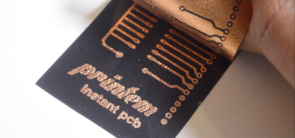
Add An Ant To Your Desk For Some Compact PCB Manufacturing

Usually when one thinks of using a CNC machine for producing PCBs, one thinks of those big, bulky CNC machines that pretty much fill an entire desk. But what if a CNC machine could be small enough to fit on a desk without getting in the way, yet still be useful enough to make single- and double-sided PCBs? This was the idea behind The Ant, the compact PCB manufacturing machine which [Mattia] and [Angelo] designed and open sourced.

In addition to the above linked Bitbucket repository for the project, the ‘Ant Team’ has a YouTube channel on which they have a range of rather professionally edited videos on the project, ranging from constructing the little machine, to various updates and more  Also see the video that is attached after the link for a visual introduction to the project.

Support and community interaction is mostly performed via the Reddit group for the project, where the diminutive machine finds a welcoming community as it continues to evolve. The machine itself is specified at this point as being able to built from commercially available and 3D printed parts, requiring no further tools for cutting or shaping. The precision is about 0.2 mm trace spacing.

Optical alignment for double-sided boards is achieved using a USB micro camera and the bCNC software, while the cost for materials is said to be quite inexpensive when compared with commercial solutions

Honestly, after seeing the machine in action, wouldn’t you want to have a CNC machine that’s so small and good-looking on your desk? If there’s one thing one might want to add, it’s probably a way to deal with the copper dust that’s produced while creating PCBs. Having to clean that off the desk after each PCB manufacturing session would get a bit cumbersome, we imagine.

Continue reading “Add An Ant To Your Desk For Some Compact PCB Manufacturing”

Friday Hack Chat: PCB Manufacturing

There’s a world of difference between building one of something and building multiples of something. The effort that goes into manufacturing does not scale linearly, and manufacturing is a skill in itself. This Friday, we’re going to be talking all about PCB manufacturing and assembly over on Hackaday.io

On deck for this Hack Chat will be [Jonathan Hirschman], the brains behind PCB:NG, a turnkey electronics manufacturing startup based around NYC. Jonathan is a self-taught hardware guy, proficient in PCB layout, 3D CAD, and manufacturing tech. PCB:NG is, essentially, taking oldskool manufacturing and making it into more of a digital process. PCB:NG makes it easy for anyone to get their designs manufactured, and to do it in the most cost-effective manner.

What is this Hack Chat going to be about? We’re going to talk about how to get started in PCB creation. What is the the best tool for the job? What is the best tool that doesn’t cost as much as a car? What are the pros and cons of each tool, and what should you know about RF before designing a board that blinks a LED?

This isn’t a Hack Chat that’s just about PCBs, though. We’re also going to be talking about manufacturing. Specifically, design for manufacturing, how to panelize boards, what happens when you forget fiducials, how to keep your designs cheap to manufacture, what happens when you put SMD components on both sides of a board.

We’re taking questions from everyone, so feel free to add something to the question sheet for the discussion.

We’re Looking For Hack Chat Hosts!

If PCB manufacturing and design isn’t your thing — or even if it is — we’re on the lookout for Hack Chat hosts. If you have some expertise in an area, give us a ring. We’ve already had a few chats with Raspberry Pi engineers, one of the brilliant people behind the ESP32, a talk on ASIC design for mixed signal oscilloscopes, and high-end audio amplifiers. We’re taking all callers, and if you have something you’d like to share with the community, send us an email. I would like to mention that it’s Burner season, and a few chats with the artists on the playa would be great, especially if they can tell us how to move the fuselage of a 747 a few hundred miles.

Here’s How To Take Part:

join-hack-chatOur Hack Chats are live community events on the Hackaday.io Hack Chat group messaging. This Hack Chat will take place at noon Pacific time on Friday, August 4th. Confused about where and when ‘noon’ is? Here’s a time and date converter!

Log into Hackaday.io, visit that page, and look for the ‘Join this Project’ Button. Once you’re part of the project, the button will change to ‘Team Messaging’, which takes you directly to the Hack Chat.

You don’t have to wait until Friday; join whenever you want and you can see what the community is talking about.

How Commercial Printed Circuit Boards Are Made

Most of us who have dabbled a little in electronics will have made our own printed circuit boards at some point. We’ll have rubbed on sticky transfers, laser-printed onto acetate, covered our clothing with ferric chloride stains, and applied ourselves to the many complex and tricky processes involved. And after all that, there’s a chance we’ll have ended up with boards that were over or under-etched, and had faults. For many the arrival of affordable online small-run professional PCB production from those mostly-overseas suppliers has been a step-change to our electronic construction abilities.

[Fran Blanche] used to make her own boards for her Frantone effects pedals, but as she admits it was a process that could at times be tedious. With increased production she had to move to using a board house, and for her that means a very high-quality local operation rather than one on the other side of the world. In the video below the break she takes us through each step of the PCB production process as it’s done by the professionals with a human input rather than by robots or ferric-stained dilettantes.

Though it’s twenty minutes or so long it’s an extremely interesting watch, as while we’re all used to casually specifying the parameters of the different layers and holes in our CAD packages we may not have seen how they translate to the real-world processes that deliver our finished boards. Some operations are very different from those you’d do at home, for example the holes are drilled as a first step rather than at the end because as you might imagine the through-plating process needs a hole to plate. The etching is a negative process rather than a positive one, because it serves to expose the tracks for the plating process before etching, and the plating becomes the etch resist.

If you’re used to packages from far afield containing your prototype PCBs landing on your doorstep as if by magic, take a look. It’s as well to know a little more detail about how they were made.

Continue reading “How Commercial Printed Circuit Boards Are Made”

This EAGLE Script Gets Quotes For Your Boards

Weary of manually entering manufacturing parameters into PCBShopper’s web form, [Jeremy Ruhland] created an awesome shortcut: His ULP script lets you obtain quotes from 26 PCB manufacturers around the world directly from your EAGLE board layout.

The script extracts all relevant data from your layout, including board size, the layer count, minimum trace widths and hole diameters. It then let’s you specify a few more in a tidy dialogue before sending you to the PCB manufacturing price comparison site PCBShopper.com with a custom query for board quotes.

It works like a charm, and [Jeremy] also plans to add a shortcut button to the EAGLE layout editor’s toolbar. Since the script implements the entire PCBShopper API, for which [Jeremy] cooperates with PCBShopper.com owner [Bob Alexander], it’s also a great starting point for the development of scripts that work with other board layout tools.

Thanks to [Matthew Venn] for the title photo (via Flickr)!

Hackaday Prize Entry: Printem Is Polaroid For PCBs

We are going to great lengths to turn a quick idea into an electronic prototype, be it PCB milling, home etching or manufacturing services that ship PCBs around the world. Unwilling to accept the complications of PCB fabrication, computer science student [Varun Perumal Chadalavada] came up with an express solution for PCB prototyping: Printem – a Polaroid-like film for instant-PCBs.

Continue reading “Hackaday Prize Entry: Printem Is Polaroid For PCBs”

Single Sided Arduino Is A Great Introduction To PCB Etching

After you’ve taken the plunge and decided to learn how to etch your own circuit boards, you’ll quickly find even the simplest boards are still out of your grasp. This is due mostly to the two-layer nature of most PCBs, and turn making a homemade Arduino board an exercise in frustration and improving your vocabulary of four-letter words.

After looking around for an easy-to-manufacture single-sided Arduino board, [Johan] realized there weren’t many options for someone new to board etching. He created the Nanino, quite possibly the simplist Arduino compatible board that can be made in a kitchen sink.

Billing it as something between the Veroduino and the Diavolino, [Johan]’s board does away with all the complexities of true Arduinos by throwing out the USB interface and FTDI chip. A very small parts count makes the Nanino much less expensive to produce in quantity than even the official Arduino single sided board.

For an introduction to etching your own PCBs at home, we couldn’t think of a better first board. As an Arduino, you’re guaranteed to find some use for it and the ease of manufacture and low parts count makes it the perfect subject for your hackerspace’s next tutorial series.

Going From Idea To Schematic To Printed PCB

Building a circuit on a bread board makes life much easier, but eventually you’re going to want a PCB for one of your circuits. Luckily, [Will] from Revolt Lab put up a trio of posts that will take you idea and turn it into a schematic and PCB.

First up is an awesome tutorial on the circuit design program Fritzing. While you won’t find Fritzing on the computer of anyone making a living doing circuit design work – those people usually go for Eagle or KiCad – Fritzing is very easy to use but still has a ton of features. Using Fritzing isn’t very hard, either. [Will]’s tutorial goes over copying your breadboarded circuit into Fritzing, creating a schematic from the bread board layout, and finally converting that to PCB artwork.

Once you have board artwork for your circuit, you’re probably going to want a real-life PCB. [Will]’s board etching tutorial goes over the toner transfer method of PCB creation. Basically, print your circuit onto glossy photo paper with a laser printer, put it face down on a copper board, then take a clothes iron to it. If you’re lucky, the laser printer toner will have transferred to the copper making a nice etch resist. To get rid of all that superfluous copper, [Will] used ferric chloride but a Hydrochloric Acid/Hydrogen Peroxide mix will work just as well.

Before you etch your boards, you might want to thing about building an etch tank that keeps all your slightly dangerous chemicals in one container. [Will]’s etch tank uses a large water container and a few pieces of LEGO to suspend the board in the etch solution. It etches boards a lot faster than laying them face down in a tray, allowing you to go from idea to finished piece a lot quicker.