A 3D Printed Junction Transistor Model

Transistors are no doubt one of humankinds greatest inventions. However, the associated greatness brings with it unprecedented complexity under the hood. To fully understand how a transistor works, one needs to be familiar with some Quantum Mechanics! As perhaps any EE undergraduate would tell you, one of the hardest subject to fathom is in fact semiconductor physics.

Take your pick: Mathematical equations governing the various currents inside a BJT

A good place to start to comprehend anything complex is by having an accurate but most importantly, tangible model at hand. Semiconductors are hard enough to describe with elaborate mathematical tools, is a physical model too much to ask?

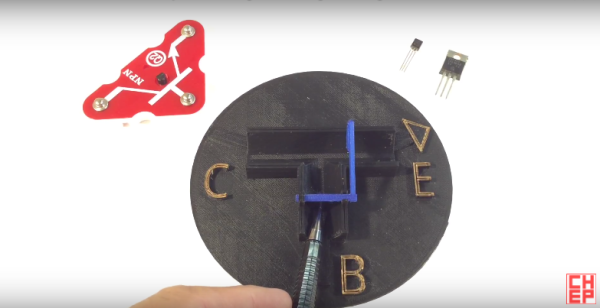
[Chuck] has designed, printed and explained the workings of a BJT transistor using a 3D printed model. We really like this model because it goes a long way to shed light on some of the more subtle features of BJT transistors for beginners.

For example, the simplest “electronic switch” model completely ignores the application of a transistor as a linear amplifier and cannot be used to explain important transistor parameters such as hfe (DC current gain Beta) or the VBE (voltage to forward bias the base-emitter junction). [Chuck’s] model on the other hand certainly offers better intuition on these, as the former can be linked to the length of the levers arm and the latter to the minimum force needed to rotate the lever. The Tee structure even signifies the combination of base current with the collector current during operation!

If physical models are not your thing, the classic pictorial depiction, the “Transistor Man” in the Art of Electronics might be of interest. If you’ve even outgrown that, its time to dig into the quantum mechanics involved.

Continue reading “A 3D Printed Junction Transistor Model”

Retrotechtacular: The Transistor (1953 Film)

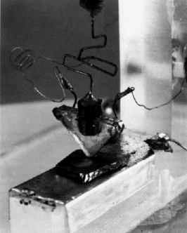
If we cast our minds back to the early years of the transistor, the year that is always quoted is 1947, during which a Bell Labs team developed the first practical germanium point-contact transistor. They would go on to be granted the Nobel Prize for their work in 1956, but the universal adoption of their invention was not an instantaneous process. Instead there would be a gradual change from vacuum to solid state that would span the 1950s and the 1960s, and even in the 1970s you might still have found mainstream devices on sale containing vacuum tubes.

First point contact transistor via kasap3

To speed up this process, Bell Labs made every effort to publicize their invention. Thus we come to our subject today, their 1953 publicity film The Transistor, in which the electronics industry of the era is described and how each part of it might revolutionize by the transistor is laid out.

We start with a look at a selection of electronic components, among which are a few transistors. The point contact device is already described as superceded by the junction transistor, but as well as those two we are shown a phototransistor and a junction tetrode, a now-obsolete design that had two base connections.

Unexpectedly we don’t dive straight into the world of transistors, but take a look back at the earlier years of the century to the development of vacuum electronics. We’re taken through the early development  and operation of vacuum tubes, then their use in long-distance radio communications, through the advent of electronics in mass entertainment, and finally into the world of radar and microwave links. Only then do we return to the transistor, with a posed shot of [John Bardeen], [William Shockley], and [Walter Brattain] hard at work in a lab. The merits of the transistor as opposed to the tube are then set out, though we can’t help wondering whether they have confused a milliwatt and a microwatt when they describe the transistor as requiring only a millionth of a watt to operate.

Continue reading “Retrotechtacular: The Transistor (1953 Film)”