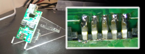
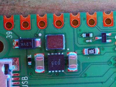
A desire for automated PCB inspection has led [charliex] down some deep rabbit holes. He’s written his own inspection software, he’s mounted his PCB vise on a stepper-controlled table, and now he’s hacked his digital microscope camera to allow remote and automated control.
Eakins cameras have become a relatively popular, relatively inexpensive choice for electronics hobbyists to inspect their small-scale work. The cameras have a USB port for a mouse and overlay a GUI on the HDMI output for controlling the camera’s various settings and capturing images to the SD card. Using the mouse-based GUI can feel clunky, though, so users have already endeavored to streamline the process to fit better in their workflow. [charliex] decided to take streamlining a few steps further.
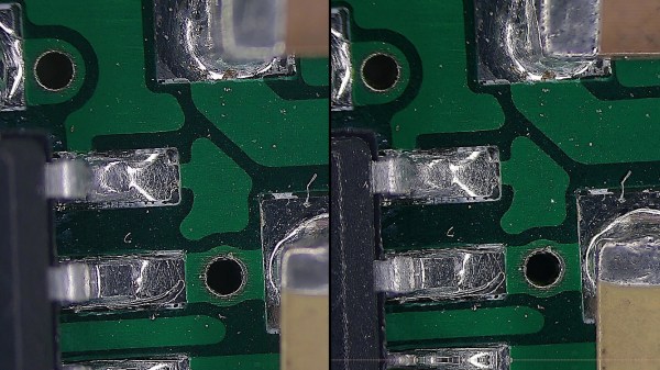
One issue in microscope photography is that microscopes have an extremely tight focus plane. So, even at the minuscule scales of an SMD circuit board, the components are simply too tall. Only a sub-millimeter-thick layer can be in focus at a time. If you take just a single image, much of what you want to see will be lost in the blurry distance. Focus stacking solves this problem by taking multiple pictures with the focus set at different depths then combining their focused bits into a single sharp image.
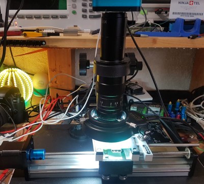
This takes care of the focus issue, but even the most streamlined and intuitive manual controls become tedious given the multitude of pictures required. So [charliex] searched for a way to remotely control his camera, automating focus stacking and possibly even full PCB scans.
Continue reading “Hacking A Digital Microscope Camera For Fun And Automated PCB Inspection”
 The principle behind this tool is as unexpected and simple as it is clever; by having different colours of light from different elevations of the dome it ensures that each different angle of the solder joint surface reflects a different colour. Thus a colour photograph shot from directly above the board allows visual inspection of the quality of the solder joints by the rainbow of colours that appears around their edges. This process can even be automated with OpenCV or similar, hence the process is referred to as Automated Optical Inspection, or AOI.