Complex programmable logic devices (CPLDs) contain the building blocks for hundreds of 7400-serries logic ICs. Complete circuits can be designed on a PC and then uploaded to a CPLD for instant implementation. A microcontroller connected to a CPLD is like a microcontroller paired with a reprogrammable circuit board and a fully stocked electronics store.
At first we weren’t sure of the wide appeal and application of CPLDs in hobbyist projects, but we’ve been convinced. A custom logic device can eliminate days of reading datasheets, finding the ideal logic IC combination, and then waiting for chips to arrive. Circuit boards are simpler with CPLDs because a single chip with programmable pin placement can replace 100s of individual logic ICs. Circuit mistakes can be corrected by uploading a new design, rather than etching and stuffing a new circuit board. CPLDs are fast, with reaction times starting at 100MHz. Despite their extreme versatility, CPLDs are a mature technology with chips starting at $1.
We’ve got a home-etchable, self programming development board to get you started. Don’t worry, this board has a serial port interface for working with the CPLD, and doesn’t require a separate (usually parallel port) JTAG programmer.
Intro to CPLDs

When to use a CPLD
Consider using a CPLD when a design calls for more than one 7400 series logic ICs. A CPLD will be cheaper, faster, and can be programmed with your ideal pin-out configuration for simpler PCBs.
Use a CPLD in tricky designs that might require several iterations. It’s easier to design a new circuit in software and upload it to the CPLD than it is to design, etch, and stuff a new circuit board.
For maximum speed and instant response, choose a CPLD. The difference in speed is amazing; CPLDs start at a 100MHz, while microcontrollers respond to interrupts at a few MHz. CPLD designs form circuits that react to external stimulus, reactions occur almost instantaneously. A microcontroller executes code to react to events, even interrupt routines have comparatively high latency.
CPLD vs FPGA
FPGAs are better known than CPLDs, but they share many characteristics. This analogy isn’t perfect, but we like it: where FPGAs are a reprogrammable processor core, a CPLD is a reprogrammable circuit board or breadboard. FPGAs replace microcontrollers, memory, and other components. CPLDs absorb logic ICs, and work well with a microcontroller.
Manufacturers
Altera and Xilinx, the biggest CPLD manufacturers, are better known for their FPGAs. Lattice Semiconductor is another large CPLD manufacturer with less community following. Atmel makes pin-compatible versions of old industry-standard CPLDs.
If you plan to work at 5volts, your options are limited. Xilinx XC9500 CPLDs are still available as new old stock, but cost four times more than newer 3.3volt equivalents. Atmel’s ATF1502 series works at 5volts, but they don’t offer a free development environment.
At 3.3volts there’s more options, but new CPLDs increasingly have a core that runs at 2.5volts, 1.8volts, or lower. The Altera MAXII and the Xilinx XC9500XL series are probably the most popular 3.3volt CPLDs. Xilinx also makes the CoolrunnerII CPLD, but it only comes in a TQFP package and requires a separate 1.8volt supply for the core.
Packages
Most manufacturers offer one or two CPLDs in a hobbyist friendly PLCC 44 package, though this is starting to disappear. PLCC is an SOIC-sized surface mount chip with pins on all four sides. PLCC44 sockets are commonly available in through-hole and SMD versions. Unfortunately, newer CPLD families are starting to eliminate the PLCC package and offer only 44 pin and larger TQFP chips, such as Xilinx’s CoolrunnerII.
Development environments
Most manufacturers offer a free development environment that supports design entry using simple schematics, as well as Verilog or VHDL. Many won’t support the latest FPGAs in the free version, but we only need the CPLD parts anyway. Altera has Quartus, Xilinx has ISE, and Lattice has ispLever. Atmel has ProChip Designer for the ATF15xx series, but they only offer a 6month trial license — which they wouldn’t actually give us.
Programmers
The development board we present doesn’t need a separate JTAG programmer because the PIC microcontroller already programs the CPLD. If you want an external programmer, the cheapest are the parallel port programmers: Parallel Cable III for Xilinx and BytleBlaster for Altera. Inexpensive clones, and schematics, are available at SparkFun. The OpenOCD is a generic USB JTAG programmer that will work with many CPLDs, FPGAs, and ARMs.
Our choice
We eventually settled on the Xilinx XC9500XL series because it had a cheap development kit we could use to test our JTAG programmer prior to implementing an entire design.
The DO-CPLD-DK from Digilent includes a XC9572XL, a CoolrunnerII, and parallel port programmer. Nu Horizons has some old non-ROHS models for $40, but due to sloppy variable type handling in their credit card processing scripts, we couldn’t complete an order online. We tried to do it over the phone but they refused to take such a small order on the phone, even during a website malfunction. In the end, it was cheaper to pay full price at Digikey (#122-1512-ND) after including New Horizon’s exorbitant shipping charges. We wouldn’t normally mention this, but with only two places to buy the board it’s probably worth noting our experience.
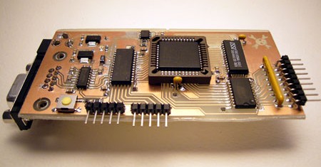
CPLD development board

Click here for a full size schematic image (PNG). The circuit and PCB are designed using the freeware version of Cadsoft Eagle. All the files for this project are included in the project archive linked at the end of the article.
Circuit
A PIC 24FJ64GA002 microcontroller (IC1) provides the user and programming interface to the CPLD. We use this $4 PIC in a lot of projects because the peripheral pin select feature makes board routing really easy. Check out our introduction to the PIC24F for more details. The PIC needs to communicate with a PC serial port, so we added an inexpensive MAX3232 RS232 transceiver. The serial interface should work with a USB->serial adapter.
Our choice of CPLD (IC3), a Xilinx XC9572XL (PDF), is connected between the PIC and several other components. We can create an endless variety of circuitry between the PIC and other chips using the reprogrammable logic inside the CPLD. The PIC will program the CPLD with code sent from a PC serial port, but we still brought the JTAG pins to a header for easy external debugging.
A DS1085 digital programmable oscillator (IC4) generates clock frequencies between 8KHz and 133MHz, at 10KHz increments. This is very similar to the DS1077 we covered earlier, but it has even steps between all frequencies. The DS1085 requires a 5volt supply (VR2). The I2C interface also runs at 5volts, so we connected it to 5volt tolerant PIC pins. It’s possible to use the 3.3volt 66MHz 1085L instead, and remove the 5volt supply.
We used a cheap 3.3volt SOT223 voltage regulator (VR1) to power most of the circuit. The 5volt supply (VR2) can be excluded if you use a slower 1085L 3.3volt oscillator.
CPLDs are commonly used as a memory controller, so we included 32K of SRAM (IC5) on the development board. A 3.3volt latch with 5volt tolerant inputs interface the memory inputs to a wide range of external voltages (IC6). The latch inputs are held low with a 1Mohm resistor network (RN1). We’ll discuss this section extensively in an upcoming article.
PCB
The board is a quasi one-sided design. We made several compromises so we could prototype this highly experimental PCB ourselves. We present the board ‘as is’ for other die-hards that might want to etch this board at home. If you send the PCB to a board house, try to correct these issues prior to producing a ‘real’ double-sided board.
One power pin of the CPLD is missing a decoupling capacitor entirely; there was no way to put a capacitor in that area. One CPLD decoupling capacitor, and the SRAM decoupling capacitor, are through-hole parts. Using these through-hole parts eliminated a few jumper wires.

The jumper wires on the back of the board are optimized for single-sided production, rather than good design practices. We faked a double-sided board by soldering the power bus on the back. A real double-sided board design should route the power bus to avoid crossing signal paths, and include the missing decoupling capacitors.
We used an surface mount PLCC chip socket, but a through-hole version is definitely a better idea. We though the SMD version would be easy to solder, but it turned out to be a nightmare. We really wanted the CPLD to be on the front of the board for the coolest possible presentation. A proper two-sided board with plated through-holes can have a through-hole socket on the front, but this wasn’t possible with our 1-sided prototype board.
Parts list

Click here for a full size placement diagram (PNG).
| Part | Value |
| IC1 | PIC25FJ64GA002 (SOIC) |
| IC2 | MAX3232CSE (SOIC-N) |
| IC3 | XC9572XL-10PCG44C (PLCC) |
| — | PLCC44 socket, SMD |
| IC4 | DS1085 or DS1085L (SOIC) |
| IC5 | 32Kx8, 3.3v, SRAM (SOJ) |
| IC6 | 74LVT573D (SOIC) |
| VR1 | 3.3v regulator, LD1117S33 (SOT223) |
| VR2 | 5v regulator, LD1117S50 (SOT223) |
| C1-11,13-17 | 0.1uF decoupling capacitors (0805) |
| C12 | 0.01uF capacitor (0805) |
| C15,16 | 0.1uF decoupling capacitors (through-hole) |
| C18 | 10uF tantalum capacitor (A) |
| R1,2 | 390ohm resistor (0805) |
| R3-5 | 2000ohm resistor (0805) |
| RN1 | 1Mohm resistor network (9 pin) |
| LED1,2 | LED (0805) |
| X1 | db9 female serial port connector *untested |
| J1 | 2.1mm power jack |
| ICSP, JTAG, SV1 | 0.1″ pin header, right angle |
| S1 | Tactile switch (DTSM-6) |
Firmware
The firmware is written in C using the free demonstration version of the PIC C30 compiler. Learn all about working with this PIC in our introduction to the PIC 24F series. The firmware is included in the project archive at the end of the article.
We wanted a super easy way to interact with the hardware on the board without endless compile-program-test cycles. We made a custom version of the Bus Pirate firmware that provides a simple ASCII terminal interface to the DS1085 clock chip (I2C), the CPLD programing interface (JTAG), and a 3 wire (SPI) interface to the CPLD. Check out the Bus Pirate tutorial for background on the simple syntax used with the firmware.
The original Bus Pirate firmware handles several protocols that share the same pins. For the CPLD version, we changed the pin assignments to fit the connections on the development board. We also removed unused modules and options.
CPLD blinky LED examples
We prepared several designs in Xilinx’s ISE development environment. The schematics, pin placement files, and compiled designs (XSVF) are included in the project archive linked at the end of the article. A full explanation of ISE is beyond the scope of this article; we found the help files sufficiently useful to make these examples.

The first design simply lights the LED connected to pin 8 of the CPLD.
Prepare the XSVF file
XSVF is a compressed JTAG programming format, as described by Xilinx in this application note (PDF). XSVF isn’t limited to programming Xilinx devices, and can be prepared for any chip that provides a common BSDL JTAG definition file.
Open the iMPACT programming tool from the ISE Design Suite project panel under Configure target device->iMPACT.
- Choose the option to create a boundary scan file, and set the type to XSVF.
- Give the XSVF output a file name and then add a compiled CPLD image (ex1.jed) when prompted to add a device.
- You should see a JTAG chain that contains a single device.

Click on the device and choose program; iMPACT will record the programming sequences to an XSVF file.
With XSVF file in hand, it’s time to open up a terminal and program the CPLD. We like Tera Term and Hercules on Windows. You must enable XON/XOFF flow control in the client to use the JTAG interface. The default PC side setting for the development board terminal is 115200bps, 8N1.
HiZ>m <–select mode
1. HiZ
2. I2C
3. JTAG
4. RAW3WIRE
MODE>3 <–JTAG
900 MODE SET
602 JTAG READY
JTAG>(2) <–probe JTAG chain macro
xxx JTAG INIT CHAIN
xxx JTAGSM: RESET
xxx JTAGSM: RESET->IDLE
xxx JTAGSM: IDLE->Instruction Register (DELAYED ONE BIT FOR TMS)
xxx JTAGSM: IR->IDLE
xxx JTAGSM: IDLE->Data Register
xxx JTAGSM: DR->IDLE
xxx JTAGSM: RESET
xxx JTAGSM: RESET->IDLE
xxx JTAGSM: IDLE->Data Register
xxx JTAG CHAIN REPORT:
0x01 DEVICE(S)
#0x01 : 0xC9 0x02 0x06 0x9A <–XC9572XL responds
xxx JTAGSM: DR->IDLE
JTAG>
In the terminal we enter the mode menu (m), and choose JTAG (3). Macro 2 probes the JTAG chain, in our case this is just the CPLD. The chain report tells us that the chip is connected and responding. Read more about the JTAG interface.

Now we can run the XSVF programmer, macro (3), and upload the XSVF file from the terminal in binary mode. The first example just lights the LED on pin 8. If the LED lights, we can verify that programming was successful. If your LED doesn’t light, don’t despair; sometimes the JTAG programmer sticks and a reset macro (1) will get the chip going.

LED at full brightness.
74LS32/4071 OR gate, blink at half rate (/2)

A major component of the CPLD development board is the 1085(L) frequency synthesizer connected to pin 7 of the CPLD. The next example uses a logic OR gate, like a 74LS32 or 4071 IC, to blink the LED whenever the clock signal is high. At even the slowest clock rate the blinking will be too fast to see, but we should get a nice PWM dimming effect compared to the first example.
JTAG>m <–select mode
1. HiZ
2. I2C
3. JTAG
4. RAW3WIRE
MODE>2 <–I2C interface to DS1085
900 MODE SET
202 I2C READY
I2C>(1) <–address search macro
xxx Searching 7bit I2C address space.
Found devices at:
0xB0 0xB1 <–found the DS1085 address
I2C>
Program the CPLD as before, and then switch to I2C mode to access the DS1085 clock. We could look up the device address in the datasheet, but we save a few seconds by running the address search macro; the report tells us the chip answers to 0xb0 (write) and 0xb1 (read).
I2C>{0xb0 0x02 0b00011111 0b10000000}<–max prescaler
210 I2C START CONDITION
220 I2C WRITE: 0xB0 GOT ACK: YES
220 I2C WRITE: 0x02 GOT ACK: YES
220 I2C WRITE: 0x1F GOT ACK: YES
220 I2C WRITE: 0x80 GOT ACK: YES
240 I2C STOP CONDITION
I2C>{0xb0 1 0b11111111 0b11000000}<–max divider
210 I2C START CONDITION
220 I2C WRITE: 0xB0 GOT ACK: YES
220 I2C WRITE: 0x01 GOT ACK: YES
220 I2C WRITE: 0xFF GOT ACK: YES
220 I2C WRITE: 0xC0 GOT ACK: YES
240 I2C STOP CONDITION
I2C>
The DS1085 is almost exactly like the DS1077 we covered earlier, but has a DAC controlled oscillator for even steps between all frequencies. We programmed the clock to the slowest frequency using the commands shown above. The LED is dimmed by the pulse-width modulation effect of the clock signal.

LED at half brightness.
74F269 16bit synchronous counter, blink slowly (/65535)

We just programmed the CPLD with a logic OR gate similar to a 74LS32. Now, we’re going to reprogram the chip with a 16bit counter like two cascaded 74F269s. At $1.15 each, two 74F269 Ics are more expensive than the XC9572XL CPLD. A 16bit counter rolls over once per 65535 ticks, so a LED attached to the last bit will toggle once every 65535/2 ticks.
Now we can see the cool part of CPLDs. The CPLD is like a programmable breadboard; we just popped out the 74LS32 and put in a 74F269, without buying parts, reading datasheets, etching, wiring, etc. A microcontroller connected to a CPLD can reconfigure its own circuit board to fix errors, add features, or re-purpose it for entirely different applications.
We upload the new design as before, but now the clock is divided by 65535 and the LED toggles about once per second.
[youtube=http://www.youtube.com/watch?v=wNfJKHV0ylg]
Taking it further
Next time we’ll look at discrete 7400-series logic chips, and implement a ton of them in the CPLD to make a high-speed bus sniffer and logic analyzer.
Download: bitclone.v1.zip


wow, great article :)
Designing logic for CPLDs and FPGAs is very similar.
Consult UC Berkeley’s EECS150 lab guides (http://inst.eecs.berkeley.edu/~cs150/fa08/Calendar.htm) for tons of detailed tutorials.
Soldering TQFP packages with an iron isn’t too bad, actually. Using lots of flux makes the job quick and clean.
CPLDs are very small, ultra low-cost FPGAs, and are definitely a great choice for a digital logic circuit. The performance gained by implementing a task-specific datapath on a CPLD and using a processor as control is incredible.
The tools have a steep learning curve, but are indeed very powerful. After learning how to use programmable logic properly, microcontrollers seem overused, and often unnecesary for many designs.
Amazing article! This seems like it would be the ideal for people wanting to learn programmable logic hardware, but more hands on.
Guys, this is awesome. I’m completely reminded of the Webserver project you put up several weeks back. Outstanding! Please keep it up!
I’d love to see something maybe leveraging the wireless space or perhaps a diy matter-antimatter reaction chamber?
The learning curve for FPGAs especially can be extremely steep, but *man* can you do cool stuff with them. I have a Spartan3 XCS1200 FPGA board that I was able to fit a complete, binary-compatible 32-processor clone of a supercomputer I found documentation for from the 1980’s =)
Making your own processor using programmable logic can be an extremely rewarding experience.
Other comapnies still making CPLDs include Actel and Cypress. Quicklogic still makes some fpga/cpld hybrid type things.
You should also mention the older and smaller PLD/PAL devices. TI still makes them, Lattice sells some, and Diodes Inc. looks like they picked up the old ICT PEEL devices.
IMHO, Using a CPLD to replace something like an 8-bit latch or a simple mux is usually a waste of money.
CPLDs are great at doing wide input functions, things like fast address decoders and counters, small state machines, picking up a few spare gates here and there, however, the registers inside them are relatively expensive because each one comes with a boatload of logic in front of it.
5V CPLDs can be a bit power hungry, especially really old stuff like bipolar 22V10s. Don’t burn yourself like I did :-)
Lattice has a decent selection of 5V parts which they acquired from AMD a long time ago.
There are now some cool analog/digital CPLD hybrid things around like cypress PSoc and Lattice POWR chips.
Atmel does seem to offer free development tools: http://www.atmel.com/dyn/products/tools_card.asp?tool_id=2759
Am I missing something?
don’t get people thinking that fpgas are _just_ reconfigurable processors. fpgas are programmable logic devices just like cplds, only much bigger and using a different internal architecture. because fpgas are much bigger you can indeed put one, two or twenty “soft processors” inside one. you can only put the simplest of processors in a cpld. you can also implement hundreds of thousands of 7400 series equivalents if you like to put it that way.
@error404
Thanks for pointing out WinCUPL, we missed it the first time. ProChip Designer is Atmel’s IDE that supports schematic entry, Verilog, VHDL, and compares to the packages offered by Xilinx, Altera, and others.
It looks like WinCUPL uses an atypical boolean language, but has a Verilog converter.
I just finished doing a design with a Lattice ispMACH4 part. Their design tools are free, too:
http://www.latticesemi.com/products/designsoftware/isplever/ispleverclassic/index.cfm?source=sidebar
You do need to buy a <$100 programming adapter to get the code into the part.
There are some very good books on using Verilog (and VHDL, but I like Verilog better) to do FPGA design. A Google search should turn them up. The ones on my shelf are _Verilog Quickstart_ by James Lee (an old ham radio buddy) and _FPGA Design with Verilog_ by Ken Coffman.
Don’t forget to check the manufacturer’s website for their docs as well. They have excellent tutorials and lists of the tips and tricks you need to know when working with each part (how to configure outputs, master clear, global clocks and all that stuff).
Start off with something simple, like a state machine to control some LEDs and move on from there. I found the hardest thing to get my head around was writing code that looked like C, but had much different rules for how it executed — all at once! It helps to think of the code blocks you write not as code, but as physical blocks in a circuit, which is what they will become.
Don’t overlook the built in simulator! It’s a bit clunky to configure, but once you get a stimulus file built, it becomes a very handy tool for checking whether your changes do what you want them to do.
Great article!
But come on, you’re not some non-technical newspaper rag. It’s MHz, not mhz. Big ‘M’ for mega & little ‘m’ for milli. Capital ‘H’ because it’s someones’ last name. Simple.
@embedded_tom : lol, I hate to point out that in your response back your entire point is made moot by the filters forcing all you capital letter to lower case.
no capital letters for you…
Great article!
@CVMagic, it is not a filter, it is just a font with all lower case. copy/paste embedded_tom’s comment to see. you can copy paste the article to see the original formatting as well.
Yes, PLEASE get that .css include fixed! Why the uppercase hate?
Specifically:
http://s3.wordpress.com/wp-content/themes/vip/hackadaycom/style.css?m=1221857817b
“text-transform: lowercase;” is listed twice. Kill it, and all the uppercase displays (yes, uppercase is stored… just not displayed. If I use firebug to kill those lines, the site looks NORMAL!)
Great article.
just wanted to add something:
one of the big (useful) differences between FPGAs and CPLDs are that CPLDs come up as soon as power is on; they don’t need to have a bitstream loaded before they can start operating.
awesome, thanks!
Actually, once you get into it, using Verilog is much easier and quicker than sketching out schematics. It’s amazing how powerful it is; an eight bit CPU (say, like a 6502) runs just a few pages of code. You can see examples on opencores.org
My own design using a CPLD is here:
http://tinyurl.com/2cemu3
Granted, I could have used a few shift registers instead of a $20 CPLD. But using the CPLD was much more interesting, and being able to “rewire” the design on the fly proved invaluable.
holy crap, you broke my brain. I was all ready and able to learn about this stuff, but this bite was WAY too big. I guess I’ll have to take smaller bites. Great in-depth article, though. I really do appreciate the painstaking detail, because it fits better with my learning style. Now if somebody could just explain to me how/why these things work, I’d be a master.
I will venture into this unknown frontier soon, I know.
regarding the lowercase thing, _everything_ here is in lowercase, see the css:
* {
text-transform: lowercase;
}
how could i not notice. the two only capital letters on this page are in “submit comment”. wow, it’s like this psychology study, where a guy ask a unsuspecting stranger for directions, they replace him with somebody else and the stranger doesn’t notice.
This is too sweet. Anyone looking into digital logic or even Crestron programming should get one of these. crestron processors are basically large versions of these
This would be a great way to run a neural net at full speed without having to build it physically.
Thanks. GOOD GOOD
Interesting read. Thanks Ian.
i dunno. i used to look at FPGA’s and cpld’s in awe like this article, but over the years I’ve come to the conclusion that they are pretty worthless for final production designs. they add to bill of materials costs, they suck up a lot of power, and with new PIC’s implementing the peripheral pin select feature, software programmable re-routing of pins is no longer a problem. if you can design your project to only use a microcontroller, you can constantly beat a cpld/fpga design over the head with lower power consumption and lower bom cost.
the only time i’d consider a fpga/cpld is if i needed something to interface at maximum speeds and where cost, power consumption, and board space is no longer an issue. however, as microcontrollers continue to get faster and integrate more high speed interface peripherals, even that reason may become dubious at some point.
hackman,
fpga’s and cpld’s are not normally used for final production. they are more commonly used for development and such until a final logic design is decided upon at which time a huge order of custom logic circuits are ordered. fpga’s name even suggests so (field-programmable gate array).
hi,
I have a xilinx XC7532XL cpld.I had sent a programme my cpld,then I could not erase this programme from my cpld.Do you know what I can erase it.
I got this look alike error message “erase protect device”
You should in stand alone erase mode.I dont know to set my cpld for this situation.
Most PLD vendors offer free tools for their low cost CPLD and FPGA families. The more recent CPLD families from Lattice and Altera are more like mini-FPGA with lots more logic than previous CPLD families.
I don’t normally comment on blogs but your post was a real help. Thank you for a great topic, I will be sure to bookmark your site and check it out again. Cheers, Amy xXx.
Is the system clock just on a general purpose I/O pin on the CPLD??
Thenk You very mutch
Thank You very mutch
Nice article :)
I’ll have to look into playing with this.
I want to do FPGA too but so far it’s been too expensive for me to get into just for playing around.
It looks like CPLD is related enough to give me some idea if I want to spend the money on FPGA and at a nice low price too.
just wanted to mention Altium are shipping an entry level fpga dev board which includes a 1 year licence to their fpga dev software for around the $400 mark, which might be worth considering as their software is great.
i need the list of commercial examples for cpld and fpga
thank you
This link: http://blog.mahalo.com/hackaday/howto/bitclone.v1.zip
doesn’t work. does anyone know where I can download bitclone.v1.zip?
Many thanks
Yeah, that link doesn’t work for me either, has anyone got a working link? Or are they able to create one for those of us that missed it and want to build one of these?
Thanks,
Steve
Great overview on CPLDs. However, I hate half standards. The JTAG interface is standardized but the connector is not. I have more than seven different JTAG cables. Of course, each device has own software :)
I have not got my software up and running to start programing the XC9572 is there a thread on building your logic circuit using the ISE software . Would be interested in seeing a few pictures of this software before i spend a few dollars in buying it .
Very well, I like this very much.
How can I get:
How-to: Programmable logic devices (CPLD)
Already assembled? If not how can I get a usable
board with all it’s documentation?
Please Advise.
Thank You
JB
Interesting. I wonder if I can aply this to my next experiment.
The link to the firmware is offline, someone please fix the link.
Thanks,
Armando
A new firmware link would be really nice since it isn’t working.
Thanks in advice, Aron
I agree. New link please :]
inspired to work a project in CPLDs…its intresting
Informative article, I loved it. Thank you more
If you want to use a cheap open source CPLD dev board check out mine here:
https://www.tindie.com/products/area0x33/areacpld/
or you can build it yourself, easy and practical for learning and some projects.
This is a terrific article (4th in Google results for “cpld” BTW, which is how I found it) and I would like to build the board, but the “bitclone.v1.zip” download at the end of the article is no longer available. Can the download link be updated?