Using 5V Programmable Logic Here In The 2020s

Do you speak GAL? [Peterzieba] does, and has pulled together a collection of documents and tools so that you can too. There’s a dividing line in electronic engineering education, between those who were taught about FPGAs, and those who weren’t. Blurring that line slightly is gate array logic (GAL). These devices were a preceursor to the FPGA, with a much simpler structure, and usually in those days UV-erasable in the same manner as an EPROM. And oddly enough, they, or at least their successor compatible parts, are still available, and as handy DIP devices that talk to 5 volt logic.

The guide goes into detail about the parts, the terminology surrounding them, and the CUPL language which raises a few memories for us. There are several possible workflows, including for those not faint of heart, the possibility of writing a fusemap by hand. We’re impressed by that one.

If these devices interest you, our colleague Bil Herd wrote a two-part guide (part one, and part two) which should answer your questions.

Thanks [Bjonnh] for the tip!

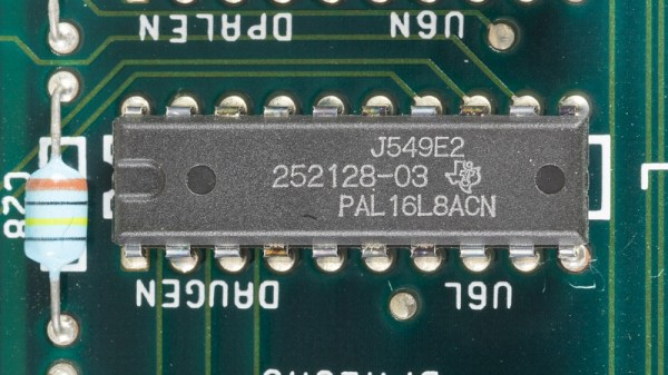
Featured image: “Commodore Amiga 1000 – sub board – Texas Instruments PAL16L8ACN-0126” by Raimond Spekking

AVR Configurable Custom Logic As A Frequency Divider At 4x Chip’s Clock Speed

What a time to be alive when you can find inexpensive microcontrollers that come with programmable(ish) logic that can operate independently of the system clock. [David Johnson-Davies] recently built a proof of concept using the Configurable Custom Logic (CCL) that is available in some of the newer AVR microcontroller designs. It’s a simple implementation, a set of frequency dividers that blink three LEDs with up to a 90 MHz input signal. But the simplicity is the reason to love his write-up — you can wrap your head around it right away.

There are four lookup table (LUTs) used to form the frequency divider. Think of these like a NAND or XOR gate, but you get to decide how the output truth tables will perform. The output is fed into a sequencer which can be configured as a D/JK flip-flop or a D/RS latch, plus you can specify the signal edge, and of course define the clock source. An interesting trick here is to hold the G input of both D flip-flops high by feeding them LUTs set to all ones. Note that the output of the first divider (PA3) is feeding the external input (PD2) of the second divider.

While the CCL is configured using the C code you flash to the microcontroller, it’s a hardware peripheral capable of operating independent of the chip’s system clock. The AVR128DA28 that’s used here tops out at 24 MHz (double that if you use the PLL) but [David] got reliable results from his clock divider feeding a signal as high as 90 MHz to the input pin. Of course you have the option of feeding internal clock signals to the CCL, but that wouldn’t seem nearly as interesting here. For the demo, [David] is actually toggling an IO pin which is connected to PA2 as the external input for the logic. Make sure you click through to his write-up linked above as he does an excellent job of walking through the sample code (just a couple-dozen lines to set this all up). Here’s the datasheet for this chip (PDF, page 447 for pertinent registers) and for a deeper dive the appnote on CCL (PDF).

So what is this all good for? We already saw an answer to that question back in January when [SM6VFZ] used the CCL peripheral to build a software-defined switch-mode converter. How awesome is that?

Hackaday Prize Entry: Very, Very Small Logic

Despite the existence of FPGAs and CPLDs, there’s still a necessity for very small programmable logic devices. GALs, PALs, and other old tech just won’t cut it, though, and so we are left with a new generation of programmable devices that aren’t microcontrollers or CPUs. The GreenPAC from Silego fill this niche quite nicely, with the ability to implement counters, ADCs, logic glue, level shifting, and comparators in a single chip. For any homebrew electronics tinkerer, these devices have one very obvious problem: they’re really, really small. The smallest GreenPAC device has 12 pins stuffed into a 1.6 x 1.6mm QFN package. You’re not hand soldering this thing.

For [Nick Johnson]’s Hackaday Prize entry, he’s taking these small programmable logic chips and making it easy to create your own custom ICs. Basically, it’s a breakout board for GreenPAC devices that stuffs these tiny chips onto a much more reasonable DIP package.

Breakouts aren’t enough, and to program these small chips, [Nick] is also building a board based on an ARM microcontroller. With USB input, a way to generate the 7.5V used for programming, and a breadboard friendly format, this programmer will tell these tiny chips what to do.

Not many people are building stuff with PALs and GALs anymore, but there are still a lot of work that can be done with small programmable chips. There’s certainly a place for tiny programmable logic chips like this, and anything that gets them in to the hands of more people is okay in our book.


The 2015 Hackaday Prize is sponsored by:

New Part Day: Modern PALs

Back in the bad old days, if you needed a little bit of custom logic you would whip out a tiny chip known as a PAL. A Programmable Logic Array is just what it sounds like and is the forerunner of modern, unsolderable CPLDs and FPGAs.

PALs and GALs have died off, left to the wastes of the Jameco warehouse, and now it seems the only programmable logic you can buy are huge, 100-pin monstrosities. [Nick] at Arachnid Labs was working on his Tsunami signal generator when a user asked if they could add just one more feature: a programmable divider to count 256 iterations of a clock. This is the perfect application for dumb logic, but if you’re looking for a part that’s not recommended for new designs, you only need to look to old programmable logic.

Enter the Greenpak. [Nick] had a dev kit for these ‘modern PALs’ sitting around and decided to give it a go. They’re small – they max out at 20 pins – but there are a few features that make it a little more interesting than a simple array of AND and OR gates. The Greenpak3 features analog comparators, look-up tables, RC oscillators, counters, and GPIO that will work well enough as circuit glue. They also work at 5V, something you’re just not going to find in more complex programmable logic.

These tiny chips are programmed in a graphical IDE, but the datasheet (PDF) includes full documentation for the bitstream; someone needs to write a Verilog or VHDL compiler for it soon. The one downside with these chips is that they’re tiny; 0.4mm pitch QFN packages. If you can solder that, you’re too good at soldering.

A Graphics Card For A Homebrew Computer

One of [aepharta]’s ‘before I die’ projects is a homebrew computer. Not just any computer, mind you, but a fabulous Z80 machine, complete with video out. HDMI and DisplayPort would require far too much of this tiny, 80s-era computer, and it’s getting hard to buy a composite monitor. This meant it was time to build a VGA video card from some parts salvaged from old equipment.

When it comes to ancient computers, VGA has fairly demanding requirements; the slowest standard pixel clock is 25.175 MHz, an order of magnitude faster than the CPU clock in early 80s computers. Memory is also an issue, with a 640×480, 4-color image requiring 153600 bytes, or about a quarter of the 640k ‘that should be enough for anybody.’

To cut down on the memory requirements and make everything a nice round in base-2 numbers, [aepharta] decided on a resolution of 512×384. This means about 100k of memory would be required when using 16 colors, and only about 24 kB for monochrome.

The circuit was built from some old programmable logic ICs pulled from a Cisco router. The circuit could have been built from discrete logic chips, but this was much, much simpler. Wiring everything up, [aepharta] got the timing right and was eventually able to put an image on a screen.

After a few minutes, though, the image started wobbling. [aepharta] put his finger on one of the GALs and noticed it was exceptionally hot. A heatsink stopped the wobbling for a few minutes, and a fan stopped it completely. Yes, it’s a 1980s-era graphics card that requires a fan. The card draws about 3W, or about two percent of a modern, high-end graphics card.

Programmable Logic I – PLA/PAL


C64-B

Yeah I am still a little pissed that the competition is still around and we aren’t, and by “we” I mean Commodore Business Machines (CBM). It was Commodore that had the most popular home computer ever in the C64 (27 Million) and it was a team of MOS engineers after all, that had the idea to make a “micro” processor out of a 12 square inch PCB.

MOS Technologies logo and address
MOS Technology in King of Prussia/Norristown

Of course they did work at Motorola at the time and “Mot” did not want anything to do with a reduction of the profit margin on the pie-plate size processor. Of course MOS got sued by Motorola but that was an average Tuesday at MOS/CBM. I absolutely credit CBM with buying the MOS Technologies chip foundry, as together we could make our own processors, graphics chips, sound chips, memory controllers, and programmable logic.

With this arsenal at our call we didn’t have to make compromises the way other companies did such as conforming to the bus spec of an industrial standard 6845 or having to add extra logic when a custom extra pin would work. We could also make sprites.

6502 Design Team
6502 Design Team (EE Times 1975, archive.archaeology.org)

The compromise we did have to make when designing was cost, and I mean the kind of cost reduction where finding a way to save a dollar ($1USD) saved millions in the production run. I knocked $.90USD out of a transformer one day and I couldn’t focus the rest of the day due to elation.

Cost reduction is a harsh mistress however as you can’t just do it a little some of the time or only when you want to. The mental exercise of multiplying anything times a million was always there, it made it hard to buy lunch — I’d be blocking the lunch line while figuring the cost of a million tuna sandwiches FOB Tokyo Continue reading “Programmable Logic I – PLA/PAL”

Reverse Engineering Programmable Logic

DickSmith_VZ300_System_s1

Despite what the cool kids are doing over on Hackaday Projects, the vast majority of vintage computers used some form of programmable logic for memory control, address decoding, and all that other stuff that can be done with just a few logic chips. It’s a great way to design a product for production, but what happens when the programmable chips go bad after 30 years?

[Clockmeister] got his hands on a Dick Smith VZ300 computer (a clone of the VTech Laser 310) with two broken 40-pin custom chips. After going through the schematics and theory of operation for this compy, he recreated the custom chips in 74 series logic.

The Dick Smith VZ300 is a fairly standard piece of equipment from 1985 – a Z80 CPU, 16k RAM, upgradable to 64k, a tape drive, and 32×16 character, 8 color display. Inside this computer are two 40-pin chips that are responsable for video buffering and VRAM control, keyboard and cassette I/O, video timing, and the monophonic speaker decoding. Both of these chips failed, and spares are unavailable, apart from scavenging them from another working unit.

After careful study, [Clockmeister] recreated the circuits inside these chip with 74 series logic chips. The new circuit was built on a board that plugs directly into the empty 40-pin sockets. Everything in this rehabbed computer works, so we’re just chalking this up as another reason why designing new retrocomputers with programmable logic is a dumb idea. Great for a product, but not for a one-off.

Image source