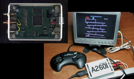
Behold [Retromaster’s] field programmable gate array implementation of an Atari 2600. The processor and video chip have both been built in the 100,000 gate Spartan-3E FPGA, with connectors for audio, video, and a Sega controller. The output signals are generated using two DACs made from R-2R resistor ladders, much like the project we saw in August. [Retromaster] included functionality for the system switches (difficulty and select) in the controller itself. There is VHDL code and board details available if you want to make one of your own. To help in making that decision we’ve embedded video of it after the break.[vimeo=http://vimeo.com/14772895]
[Thanks Gokhan]


Hoorj!
A Sega controller? But why?
Because the Sega controller is pin-compatible with Atari joysticks. You can actually use an unmodified Genesis controller with an Atari 2600.
I attend Washington State University and in my EE 214 (Logical Circuits) Class, in a previous semester, someone implemented a super nintendo with a Spartan 3E FPGA board.
It was pin compatible, and it did work (on the c64 and coleco vision too!), but only the dpad and B button worked — it mapped to button 1 basically on the other two consoles, or the main button on atari.
A, C and Start (and later mode, X, Y, and Z) you had to send a special signal to read… so the atari and older hardware couldn’t work with them.
It sounds like though, he’s actually using all of the buttons on the Genesis controller — they do the functions the switches did on the real 2600 (set difficulty, etc).
@Taylor most of the specs for all this stuff is up for grabs on the internet, I can’t imagine doing any of it in an FPGA is that difficult…
I think that the Sega controller is a good choice, because:
1. Enough buttons.
2. Standard DB9 connector.
3. Very easy to implement, much simpler than a USB gamepad.
4. Brand new controllers very cheaply available on ebay.
5. Original Genesis controller quite comfy, IMO.
I guess that’s enough… If not, VHDL sources are available so anyone can implement their own choice of controller :)
This is very impressive work. It takes a lot of dedication to get a complex system like this fully debugged in FPGA.
@Taylor Cox: I don’t believe it. The snes is a horribly complex beast (16-bit cisc, separate DSP, multiple busses) and there’s no way it would all fit in an FPGA unless perhaps it was being software emulated. Even then I doubt a 100MHz or so DLX which is about the best you can hope to achieve on a Spartan 3E would be anywhere near adequate for snes emulation. Did you actually see it?
@svofski: Superior job, old bean!
@Mikey
I’m quite sure you’ve never worked with an FPGA before. You should know that the timing is VERY critical and the whole designing process is completely different to software development that you seem to do. Imagine a system where everything is running in parallel and just 1 signal is a clock cycle too late… I agree with nes, it’s very impressive to rebuild an “old” processor in an FPGA fighting with the bugs and the timing of the original machine.
I don’t get why u just don’t use a parallel propeller!? The prop is the best uController
I’d love to see someone adapt this for DVI/HDMI output. Composite video sucks. I want to see perfectly sharp graphics in all their blocky glory. Digital sound would be neat too.
Taylor is very probably referring to an FPGA NES clone that a friend and I developed while at WSU a few years ago (some limited details are on my website: http://danstrother.com/fpga-nes/ ). But we made a regular NES – not a SNES (and, in the interest of being exorbitantly pedantic: it was in EE324 with a regular Spartan-3, not EE214 with a 3E).
Now, if someone *has* actually gone and implemented a SNES in an FPGA, then I would be truly impressed! We briefly considered it after getting our NES working, but @nes is quite right in asserting that it would be a huge undertaking. Not impossible, mind you, but vastly more difficult than a regular NES – owing partly to just the increased complexity, but more-so owing to a lack of good documentation about the very low-level details of the SNES chips (rather than having a nice cycle-accurate description of each chip’s internal behavior to implement from, you have to actually do some real serious design work to correctly implement all of the externally-visible behavior). I’m sure you could fit it in a moderately sized FPGA, however – the SNES isn’t *that* much more complex than a regular NES.
And, @Retromaster: awesome work! Fitting all of that in a 100K gate FPGA is certainly a feat, and major kudos for writing the 6502 from scratch – that’s something I’ve been wanting to do for quite some time (for now, I’m relying on a core from OpenCores).
The original TIA IC schematic was hand drawn (like most other ICs at the time), which was quite interesting. I have a scan of those somewhere on my machine. Should dig them up someday for a closer look.
Someday never comes ..
What about player 2???