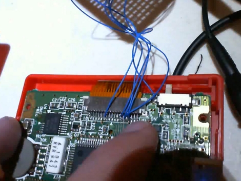
[ViDAR] was looking for a project to keep him occupied and settled on creating a VGA converter for his Game Boy. He had some difficulty finding pinouts for the LCD and CPU but working with what was known, and an oscilloscope, he found the necessary signal. Tap into just a few lines using those thin blue wires; Vsync, Hsync, clock, and two data pins. From there a development board with an Altera Cyclone II field-programmable gate array takes care of the heavy lifting. The board already has hardware for a VGA connection so it was just a matter of processing the incoming signals into the VGA standard. His demo video is embedded after the page break.
Want a dedicated solution? Check out this Game Boy video adapter inside a VHS cassette.
[youtube=http://www.youtube.com/watch?v=NUIWsUHntf8&w=470]


what cant FPGA’s do? XD
*cough*
Nice acrylic cover on his DE1. I wontie
Hmm, GameBoy Pocket to VGA. Man, if it were only the early 90s, that would be a state-of-the-art hack. How about something more current, like Nook Color to HDMI?
I’m just joking btw, great work, love the Logitech stereo (I have the same one) and please get some cough drops and a better camera.
King of the blurry Cam, and it sounds like he has a cold too. :(
that being said this is really cool. I want some fgpa skillz.
The high pitched sound coming from the webcam’s mic, his constant coughing in the mic, and the shakiness of the video killed it for me. Awesome project though.
couple of years late on this mod but a great POC none the less.
+1
I just spent most of the weekend getting a PIC to talk to a color LCD from an old Nokia cell phone (3510i). I feel inferior.
Soldering to those pins looks like a real bitch. I recently just soldered up one of those Nokia 3310 LCDs to a ribbon cable and that took me forever.
For people who cbf doing this hack and want any kind of handheld on the big screen theres always emulators. Ahh I remember in primary school we’d all be playing pokemon roms on the school computers.
It’s not just the FPGA but the analyzing the signals, impressive, this is certainly not going to get a ‘that’s not a hack’ post :)
not a hack..
BiOzZ: most companies design new CPUs by coming up with some VHDL and loading it onto a (very expensive) FPGA. I’m not sure if Intel still does it this way, but I have heard that they used to load some of their fastest intel processors (think Pentium 4) onto FPGAs.
http://www.8051projects.net/lofiversion/t37003/mobile-controlled-robot.html
@tulcod
You’d need a very very big FPGA to get a whole P4 into it… and those sort FPGA’s have PPC cores ;P. It’s very possible Intel developed/develops their stuff in some HDL and simulates the designs. If they didn’t they’d have a lot of wasted silicon.
Look up the Ferranti ULA (this book is pretty good http://www.zxdesign.info/book/theZXSpectrumULA.shtml — the first couple chapters are all about the Ferranti ULA..). It was ground breaking in it’s time.
fpga’s are easy, you just have a cliff learning curve.
Get off your butts, get the stuff needed to program them and get learning people~!
@tulcod: Yes they do but they’re typically using a whole box stuffed with FPGAs as gate-level simulator. The FPGAs will be running fixed configs which include simulating some gates and a big switch matrix for hooking up signals to their neighbours. It runs the design much slower than realtime but it’s still quicker than you can simulate in software.
This is opposed to partitioning up your 10s of millions gate CPU design into hundreds of chunks and mapping each one to an FPGA individually which would take a lot of computer time (and puts a lot of faith in the FPGA vendor’s software).
@fartface
VHDL isn’t too bad if you have some understanding of logic and have used parts out of the 74 series or something. If you get into you head that you are describing some hardware you want and not programming an application you can start to think in VHDL really quickly.
The great thing is that you make something that looks like a ROM in VHDL and the toolchain goes “hey, that looks like a ROM to me, going to make that a ROM buddy, that’s a counter isn’t it?.. That looks like RAM, so I’ll do you a favour and implement that with Block RAM matey”.
The bad things from my experience are everything is 3.3v or lower.. if you want to interface to stuff running at 5v that can be a pain if the bus is bi-directional. I have processor boards, sound generators etc that I wanted to hack together with my FPGA board to make a retro console but I soon gave up when I realised all I’d have to make a ton of buffer daughter boards to interface them. The tools have proprietary written all over them, the best tools are on Windows.. you can get Xilinx’s ISE to run on Linux but it’s a bit clunky.. and then your dev board probably has some proprietary programming interface that needs Windows software to use or you have to buy a supported (read: expensive) JTAG dongle to use your board. I was working with ISE on Debian and uploading bitstreams to my Digilent Nexys2 via a Windows XP VM for a long time… The build, upload, test cycle was incredibly painful. Digilent has released linux interface drivers that plug into Xilinx’s tools now which made everything a million times more useful.
Please get a stand for that camera, and please don’t record any videos until you don’t cough that much…
Seriously guys, so yeah he has a bit of a cold, in winter, and it’s a handheld webcam, but I’ve seen so much worse and that includes professional efforts and prime time shows and even movies with more shaky shots that do actually make you nauseous, this is nowhere near that.
And he’s obviously trying to not cough and excuses himself for the cam, what more do you want?
Chalk me down as being fine with this video.
Internet Tip: try to make sure that less than 60% of your comments are 100% bitching complaints ;)
HAD -> PLZ moderate all comments or force registration.
@Cantido – the tools are smart, but for them to infer hard blocks like you are talking about sometimes takes “finessing” the code, to say the least, and sometimes takes explicitly telling the synthesis tool that you are creating a hard block. Case in point, I can get synplify and ISE to infer BRAM only if I add the syn_ramstyle=”block_ram” attribute to the array signal I am using as memory. Other times, you have to write the code juuuust the right way for it to understand that you are invoking a hard block. Its definitely not as simple as it could be :-/
@HADViewer <- agree.
@fartface – agreed. I think this project is the one that finally gets me off my butt. I’ve been meaning to buy an FPGA development kit for years…
To the folks thinking of starting out with FPGAs: it is possible get by without learning any VHDL or Verilog to start with. Most (all?) of the FPGA vendors’ tools have the option of schematic capture where you have a limited parts library of logic gates, registers, RAMs, simple math functions and so forth which you just hook together as you would real components.
Draw your circuit, figure out a list of which physical pins on the FPGA you want to use, hit go and the tools magically turn it into a file you download to the FPGA. It’s not the quickest way to design something but it might soften the learning curve a bit.
@nes
Verilog looks a lot like C code, but if you write Verilog like C you will have a synthesized design that is an insane Rube Goldberg implementation of the algorithm you intended. FPGAs are as close to an ASIC as you can get so when you use hardware description languages make sure you have hardware in mind.
FPGA’s are awesome. Now all he needs to do is upscale the resolution to 1080p + anti-aliasing.
@Gert
Sounds like you are looking for a Gameboy emulator.