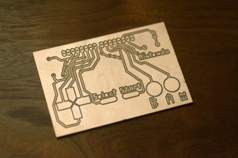
Here’s one way to really keep the component count low. [David] developed an NES controller that doesn’t use any buttons. The copper clad has been milled to provide a pad which registers a button push based on capacitance. The board has a SIL header at the top, making it easy to plug into the Arduino board that reads the inputs.
[David] had trouble getting the Arduino pin read functions to respond fast enough for he NES console’s expectations. He ended up using commands to access the ATmega’s peripherals directly in order to achieve the target timing. Speaking of, he did his own sniffing of the communication scheme using a logic analyzer. The results of that work, as well as the board files and code are available at the site linked above. And there’s a demo of the controller used to play Super Mario Bros. in the clip after the break.
This is actually a tangential project using a PCB mill which he’s developing through Kickstarter. This certainly shows that the mills works as designed. [youtube=http://www.youtube.com/watch?v=q77DB5VSVzI&w=470]


I want a whole keyboard like that, that is awesome.
Ah ha! I hadn’t realized his CNC mill was targeted at PCBs. I had questioned the usefulness when his intro video merely showed some light wood engraving. Now, I’m much more impressed with its utility.
Wow, that’s very clean milling! Sadly, I don’t see the kickstarter succeeding :(
At least there’s ShapeOko:
http://www.kickstarter.com/projects/edwardrford/project-shapeoko-a-300-complete-cnc-machine
Very steampunky.
Too bad he didn’t find the NES-compatible SNES controller source code from this year-old article.
Damn, have to try this at some point :) CNC is waiting for something to run.
This guy dropped in to visit the ATX hackerspace recently. He totally should have brought this board along, or had his mezzomill cut one out.
At least it probably works better than the TurboTouch 360 did. Because god knows it can’t be WORSE.
Yes, this is at least the SECOND capacitive NES pad design. :P
It’s a cool process and I get the message he’s trying to pass off here. What I don’t get is why go through the trouble of tacking on a logic analyzer to an NES controller?
The datasheet for the 4021 would have told him everything he needed to know and then some.
Was he just practicing his analyzer voodoo?
I’ve found cap-touch sensors to be buggy. Sometimes they work sometimes not, sometimes they work when you don’t want them to. Hmmm… Maybe it’s my code – but I don’t think so.
¿Really? I’ve found they are very reliable as long as the item they are sensing (e.g. the body of the user) is properly grounded.
Of course – stupid me for not connecting my body securely to a ground connection before touching a piece of electronic equipment (and I don’t mean a hi-z wrist strap).
Common household appliances (computers, fridges, washing machines) have their enclosures connected to ground, and you can touch them, right?
Isolate the contact pads with a layer of plastic, and surround them with a grounded trace.
While I love the idea of hacking and projects that include capacitive touch, the thought of this makes me squirm.
Playing the SNES is something that requires you to keep your eyes on the screen and not on the controller. Without buttons you have little to no tactile feedback when you start mashing and will easily slip, spoken from experience playing mario on my phone using a controller overlaid on the touchscreen.
Fantastic work, but in my opinion a very impractical idea!
I was actually just about to chime in and moan about buttons without tactile feedback. :P
Thanks for pretty much covering everything I was going to say. :p
This is more a novelty then a usable product. It’s something for fun. “Hey, want to play super mario without buttons!?” It’s like a giant controller, fun, but not for hardcore gamers.
Is this as accurate as an iphone touch screen?
No. It can’t be! There is NO ‘i” in front of NES controller.
Was the video faked? The game paused without pushing the start button.
I think his thumb probably grazed the start trace or something to that effect. The controller is quite small in comparison to an actual NES controller, so it’s more than possible he grazed it.
too bad his PCB mill is way overpriced compared to alternatives like ShapeOko and MyDIYCNC.com
I’m familiar with this project. The guy who makes it hasn’t done a great job ‘selling’ the idea.
What he really wanted was a PCB printer which would work as simply as a normal printer. It’s non-trivial to go from a general purpose CNC machine to producing quality PCBs as anyone who has done so can tell you. It can take weeks and months of time to produce good boards. There are lots of steps and lots of trials and experimentation that you need to do go get it working. The software for his machine takes out that complexity. You make a PCB in eagle using his template then it does the rest for you after pushing a button. Even a novice can produce a PCB very quickly.
To do this, he had to add lots of stuff to the project like automatic homing and a custom machined fixture to hold the PCBs in a consistent location for cutting. It all adds up the cost. He is also constructing them himself in tiny quantities which is expensive. Then there is all the software work he did.
So, yes, you can do everything he is doing for less money yourself, or by a CNC router kit, but his solution works out-of-the-box which is the whole point. It’s designed for people who want to produce PCBs, not for people who want a CNC machine project.
My point is that you can’t strait compare the prices between this and a general purpose CNC kit.
I like how the labels for the buttons and the logo in the corner spell out “BAM”. ;)
It’s worth noting that there’s a quite recent technology, which I had the pleasure to write a paper about, that is called “Molded Interconnect Devices”: basically you can print circuitry on plastic.
The way it works is that you take a special palladium (or other noble metal) doped thermosetting polymer, mold it to whatever shape you want, laster etch the circuit path on in to expose the noble metal and let it marinate in an electroless copper bath for a couple of minutes so that it would attach on the etched circuitry: you just made a MID.
I’ve seen capacitive and resistive buttons, chips, resistors and LED’s soldered on the MID frame… looks like the picture above but you can do way more complex stuff.
Cool! I’ll run down to my corner drugstore and pick up a pack of palladium doped thermosetting polymer. :)
Don’t forget the YAG laser and couple of copper ions.
Can you pick me up a can of plutonium while you’re out?
What is this style / technique of PCB called? where you leave most of the copper on?
It’s an amazing piece of writing in support of all the web visitors; they will obtain advantage from it I am sure.