Learning to lay out a printed circuit board takes some time. But after you’ve churned out a few it’s really pretty easy. If you find yourself at that point it may be time to learn about more complicated board fabrication. We think a good primer is this multi-layer PCB layout guide which [Rik te Winkel] recently put together. It’s one of the results of his internship experience.
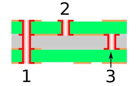
One of the major differences with boards that have more than two layers is the ability to alter what layers are actually connected by vias. Vias are plated holes through the substrate that connect different layers of copper. In the case of a 2-layer board these just go right through and connect the top to the bottom. But as you can see above, there are additional choices when it comes to multi-layer boards. #1 is a through via connecting all of the layers. #2 is a blind via; it stops part way through the board. And #3 is a buried via; it connects internal layers but cannot be seen from either side.
The guide is aimed at Eagle CAD. To use more than two layers you’ll have to purchase a license. But we think the concepts can easily be translated to other PCB layout software like Kicad.


For any commercial use you also need to buy an EAGLE license, but for the Light version it is only around 50€ compared to few hundred for the versions supporting more layers.
Still would like to get one of the multi-layer versions :P
Blind via (2) are prone to failure during the plating process. Boards are moved from side to side so that plating solution makes it into the holes each time the boards move. If the hole is only open on one side the plating solution in the hole will be spent very quickly, resulting in poor quality. Also buried vias (3) would make your board at least twice as expensive to produce.
As an alternative stick to full thru hole via.
p.s. I made PCB’s from 1986 till 1994, but I don’t think things have changed that much.
i want to learn pcb designing but i do know from where should i learn the same
Yeah, I bought the hobby version and it has been great. Haven’t tried multi-layer boards but the larger board size is awesome! I’ll probably be doing multi-layer stuff soon though, so this tutorial looks great!
KiCAD is much superior to Eagle.
Unless you try to use it. EAGLE doesn’t have the best user interface. But it’s a LOT easier to use then KiCAD.
I teach graphical user interface design and human computer interaction classes at a university. KiCAD is the best example I have for what not to do. Everything about that program is a horrible unintuitive mess to use. It’s not user friendly… it’s actually user abusive.
Having blind and/or buried vias will substantially change the board yield (per the previous comment) and hence the true cost. Depending on the fabrication house you may pay more, or not, depending on if you get all the boards or just the functional ones. That said, if space is limited there is nothing like “building up” rather than “out” to make the needed routes.
I’ve got to agree with the above comments, unless you really need to use blind/buried vias, it’s best to avoid them.
I will say this, I’ve seen A LOT of 4-layer designs in my time that have not needed 4 layers. There are times when it is unavoidable, but I’ve taken designs that people (admittedly, guys that are new to layouts) have thought had to be done with 4 layers and brought them down to 2 in the same amount of board space (and often times less).
KiCAD is a very nice tool, although I caution those who love ground planes/pours (like me), KiCAD does not auto cut clearance for pours, you have to tell it to cut clearances before you generate your CAM files (at least it used to do this). I had to almost scrap a board once as I ran a power line to a part and forgot to ‘redraw’ the ground pour in that area and ended up with a short that took hours to track down…
Never was a bit fan of Eagle, although it is a very popular tool.
For people that don’t need schematic integration, FreePCB is a very easy took to use and produces some very nice quality work. I use it almost exclusively. I pair it with the Orcad for schematics (use the 9.1 student version that is out there) and that takes care of 99.1% of my needs. The other 0.1% things like RF boards where I use Microwave Office, ADS, or good ‘ol Cadence Allegro…
I currently lay out PCBs for my job and have done a couple courses on best practice
What has been said is correct, buried and blind vias do increase cost considerably (although costs are slowly coming down). Its usually cheaper to have vias that go all the way through, but these more expensive methods may be necessary where you have high chip densities, especially when using BGA chips or where high layer counts have become necessary.
When PCBs go up to very high layer counts (16+), such as PC motherboards, buried and blind vias also become necessary, as through hole vias will end up filling your signal layers, making routing nearly impossible.
Its usually cheaper (and more reliable) to slightly increase your board size and avoid these expensive vias.
Also its not always best to reduce layer counts; 4 and 6 layer boards do not cost much more than 2 layer boards and may allow you to reduce board size considerably (saving money), not to mention signal integrity, which will always be much, much better on boards with 4 or more layers. This is especially important when dealing with mixed signal PCBs (analogue and digital) as you need low impedance power and ground planes.
Some very informative comments.
Thank you guys :)
Does anybody have a tip where to get cheap 4 Layer boards?
For 2 Layers there are quite a few offers such as seeed studio, itead or dorkbot, but i haven’t found anything goood for 4-6 layers yet. If I use “normal” production houses the price quickly goes from 1-10$ for a 5cm * 5cm board to 50-100$.
It really depends on where you are, what quantity you want, what spec you’re after (track and gap widths, quality of finish, testing etc).
There are a few production houses over in the east that can do very cheap reasonable quality boards with reasonable turnaround time in low to medium quantities.
The cheapest pcbfab for multilayer I know is http://www.pcbya.com.
You may take a look at the Edadoc PCB services:
http://en.edadoc.com
They offer both design and manufacturing services with great pricing and high quality service.
Dorkbot does 4-layers ($10/(3x 1-sq in)), instead of $5.
I have only used there 2 layer service, but they are fast and reasonably priced.
http://www.expresspcb.com/
Ya if you need to use blind and buried vias, you already know about them and how to use them and you don’t care about cost. I’ve done really complex 4+ layer boards and never once used blind or buried vias. If you use stuff like blind/buried vias, super tiny traces/clearance, super tiny holes, or anything exotic like that the cost is going to go up big time and the board houses that can do the job (well) will become fewer.
The main reason to go 4+ layer is you need to put components on both sides, and still keep good ground/power planes. Having the extra routing layers is nice too. All this isn’t taking into account specialty designs like RF stuff or huge BGAs, where you might not have any other choice.
Quote from top post: “Learning to lay out a printed circuit board takes some time. But after you’ve churned out a few it’s really pretty easy.”
You can’t “churn out” PCB designs. If you do then you’re not doing it right. There’s *a lot* more to PCB design than just throwing parts and tracks down onto a bit of copperclad. Especially at the level of complexity where you’d consider using blind and buried vias.
The challenge of PCB layout is the attraction for me, many people enjoy the NP-Hard problems it presents and the amount of planning required to create an elegant and robust design within budget and within deadline.
Easy it is not. :)
Updated links to the guide
http://www.brc-electronics.nl/component/kunena/10-Contributions/193-Using-Eagle-for-multilayer-PCBs-4-or-more-layers?Itemid=0
http://brc-electronics.nl/Generalfiles/Report2.pdf
The link in the article is broken.